MS18R1622(4/8)DH0
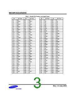
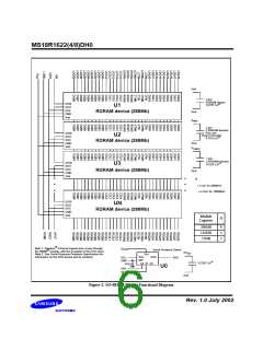
Table 3 : Module Connector Pad Description
Signal
Pins
I/O
Type
Description
A1, A3, A5, A7, A9, A11, A13, A15,
A17, A19, A21, A23, A25, A27, A29,
A31, A33, A37, A48, A50, A52, A54,
A56, A58, A60, A62, A64, A66, A68,
A70, A72, A74, A76, A78, A80,
B1, B3, B5, B7, B9, B11, B13, B15,
B17, B19, B21, B23, B25, B27, B29,
B31, B33, B37, B48, B50, B52, B54,
B56, B58, B60, B62, B64, B66, B68,
B70, B72, B74, B76, B78, B80
Gnd
Ground reference for RDRAM core and interface. 72 pins.
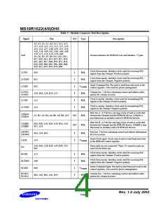
Clock from master. Interface clock used for receiving RSL
signals from the Channel. Positive polarity.
LCFM
B10
I
I
I
I
I
I
RSL
RSL
Clock from master. Interface clock used for receiving RSL
signals from the Channel. Negative polarity.
LCFMN
LCMD
B12
Serial Command Pin. Pin used to read from and write to the
control registers. Also used for power management.
B32
VCMOS
RSL
LCOL4..
LCOL0
Column bus. 5-bit bus containing control and address infor-
mation for column accesses.
A18, B18, A20, B20, A22
Clock to master. Interface clock used for transmitting RSL
signals to the Channel. Positive polarity.
LCTM
A12
A14
RSL
Clock to master. Interface clock used for transmitting RSL
signals to the Channel. Negative polarity.
LCTMN
RSL
Data bus A. A 9-bit bus carrying a byte of read or write data
between the Channel and the RDRAM device. LDQA8 is
non-functional on modules with x16 RDRAM devices
LDQA8..
LDQA0
A2, B2, A4, B4, A6, B6, A8, B8, A10
I/O
I/O
RSL
RSL
Data bus B. A 9-bit bus carrying a byte of read or write data
between the Channel and the RDRAM device. LDQB8 is non-
functional on modules with x16 RDRAM devices.
LDQB8..
LDQB0
B30, B28, A30, B26, A28, B24, A26,
B22, A24
LROW2..
LROW0
Row bus. 3-bit bus containing control and address information
for row accesses.
B14, A16, B16
A32
I
I
RSL
Serial Clock input. Clock source used to read from and write
to the RDRAM control registers.
LSCK
NC
VCMOS
A36, B36, A38, B38, A40, B40, A41,
B41
These pads are not connected. These 24 connector pads are
reserved for future use.
Clock from master. Interface clock used for receiving RSL
signals from the Channel. Positive polarity.
RCFM
RCFMN
RCMD
A71
I
I
I
I
RSL
RSL
Clock from master. Interface clock used for receiving RSL
signals from the Channel. Negative polarity.
A69
Serial Command Input. Pin used to read from and write to the
control registers. Also used for power management.
B49
VCMOS
RSL
RCOL4..
RCOL0
Column bus. 5-bit bus containing control and address infor-
mation for column accesses.
B63, A63, B61, A61, B59
Rev. 1.0 July 2002
Page 3

 SAMSUNG [ SAMSUNG ]