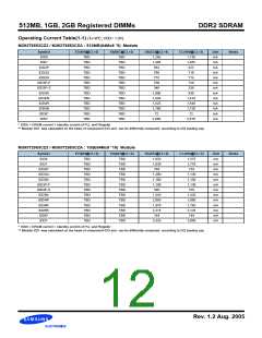
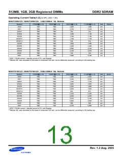
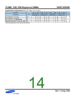
512MB, 1GB, 2GB Registered DIMMs
DDR2 SDRAM
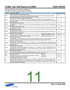
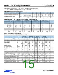
IDD Specification Parameters Definition
(IDD values are for full operating range of Voltage and Temperature)
Symbol Proposed Conditions
Units
Notes
Operating one bank active-precharge current;
CK = CK(IDD), RC = RC(IDD), RAS = RASmin(IDD); CKE is HIGH, CS\ is HIGH between valid commands;
Address bus inputs are SWITCHING; Data bus inputs are SWITCHING
t
t
t
t
t
t
IDD0
mA
Operating one bank active-read-precharge current;
t
t
t
t
t
t
t
IOUT = 0mA; BL = 4, CL = CL(IDD), AL = 0; CK = CK(IDD), RC = RC (IDD), RAS = RASmin(IDD), RCD =
IDD1
mA
t
RCD(IDD); CKE is HIGH, CS\ is HIGH between valid commands; Address bus inputs are SWITCHING; Data pattern
is same as IDD4W
Precharge power-down current;
All banks idle; CK = CK(IDD); CKE is LOW; Other control and address bus inputs are STABLE; Data bus inputs are
FLOATING
t
IDD2P
IDD2Q
IDD2N
IDD3P
IDD3N
t
mA
mA
mA
Precharge quiet standby current;
t
t
All banks idle; CK = CK(IDD); CKE is HIGH, CS\ is HIGH; Other control and address bus inputs are STABLE; Data
bus inputs are FLOATING
Precharge standby current;
t
t
All banks idle; CK = CK(IDD); CKE is HIGH, CS\ is HIGH; Other control and address bus inputs are SWITCHING;
Data bus inputs are SWITCHING
Active power-down current;
mA
mA
Fast PDN Exit MRS(12) = 0mA
t
t
All banks open; CK = CK(IDD); CKE is LOW; Other control and address bus
Slow PDN Exit MRS(12) = 1mA
inputs are STABLE; Data bus inputs are FLOATING
Active standby current;
t
t
t
t
t
t
mA
mA
All banks open; CK = CK(IDD), RAS = RASmax(IDD), RP = RP(IDD); CKE is HIGH, CS\ is HIGH between valid
commands; Other control and address bus inputs are SWITCHING; Data bus inputs are SWITCHING
Operating burst write current;
t
t
t
t
t
All banks open, Continuous burst writes; BL = 4, CL = CL(IDD), AL = 0; CK = CK(IDD), RAS = RASmax(IDD), RP =
IDD4W
IDD4R
t
RP(IDD); CKE is HIGH, CS\ is HIGH between valid commands; Address bus inputs are SWITCHING; Data bus inputs
are SWITCHING
Operating burst read current;
t
t
t
t
All banks open, Continuous burst reads, IOUT = 0mA; BL = 4, CL = CL(IDD), AL = 0; CK = CK(IDD), RAS = RAS-
mA
mA
t
t
max(IDD), RP = RP(IDD); CKE is HIGH, CS\ is HIGH between valid commands; Address bus inputs are SWITCH-
ING; Data pattern is same as IDD4W
Burst auto refresh current;
t
t
t
IDD5B
IDD6
CK = CK(IDD); Refresh command at every RFC(IDD) interval; CKE is HIGH, CS\ is HIGH between valid commands;
Other control and address bus inputs are SWITCHING; Data bus inputs are SWITCHING
Self refresh current;
CK and CK\ at 0V; CKE ≤ 0.2V; Other control and address bus inputs are
FLOATING; Data bus inputs are FLOATING
Normal
mA
mA
Low Power
Operating bank interleave read current;
All bank interleaving reads, IOUT = 0mA; BL = 4, CL = CL(IDD), AL = RCD(IDD)-1* CK(IDD); CK = CK(IDD), RC =
t
t
t
t
t
IDD7
t
t
t
t
t
t
t
mA
RC(IDD), RRD = RRD(IDD), FAW = FAW(IDD), RCD = 1* CK(IDD); CKE is HIGH, CS\ is HIGH between valid
commands; Address bus inputs are STABLE during DESELECTs; Data pattern is same as IDD4R; Refer to the follow-
ing page for detailed timing conditions
Rev. 1.2 Aug. 2005

 SAMSUNG [ SAMSUNG ]