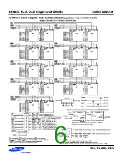
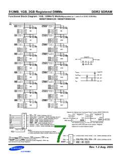
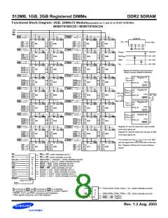
512MB, 1GB, 2GB Registered DIMMs
DDR2 SDRAM
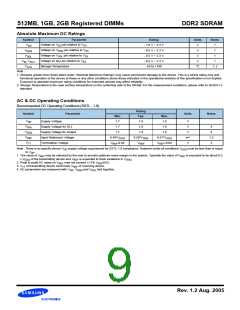
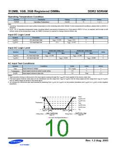
Operating Temperature Condition
Symbol
Parameter
Rating
Units
Notes
TOPER
Operating Temperature
0 to 95
°C
1, 2, 3
Note :
1. Operating Temperature is the case surface temperature on the center/top side of the DRAM. For the measurement conditions, please refer to JESD51.2
standard.
2. At 85 - 95 ×C operation temperature range, doubling refresh commands in frequency to a 32ms period ( tREFI=3.9 us ) is required, and to enter to self
refresh mode at this temperature range, an EMRS command is required to change internal refresh rate.
Input DC Logic Level
Symbol
(DC)
Parameter
Min.
+ 0.125
Max.
V + 0.3
DDQ
Units
Notes
V
DC input logic high
DC input logic low
V
V
V
IH
REF
V (DC)
- 0.3
V
- 0.125
REF
IL
Input AC Logic Level
DDR2-400, DDR2-533
Min. Max.
+ 0.250
DDR2-667, DDR2-800
Symbol
Parameter
Units
Min.
V + 0.200
REF
Max.
V
(AC)
AC input logic high
AC input logic low
V
-
V
V
IH
REF
V (AC)
-
V
- 0.250
V
- 0.200
REF
IL
REF
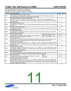
AC Input Test Conditions
Symbol
Condition
Value
0.5 * V
Units
V
Notes
1
1
V
Input reference voltage
REF
DDQ
V
Input signal maximum peak to peak swing
Input signal minimum slew rate
1.0
1.0
V
SWING(MAX)
SLEW
V/ns
2, 3
Notes:
1. Input waveform timing is referenced to the input signal crossing through the V
(AC) level applied to the device under test.
IH/IL
2. The input signal minimum slew rate is to be maintained over the range from V
to V (AC) min for rising edges and the range from V
to V (AC)
REF IL
REF
IH
max for falling edges as shown in the below figure.
3. AC timings are referenced with input waveforms switching from V (AC) to V (AC) on the positive transitions and V (AC) to V (AC) on the negative
IL
IH
IH
IL
transitions.
V
V
V
V
V
V
V
DDQ
(AC) min
IH
IH
(DC) min
V
SWING(MAX)
REF
(DC) max
IL
IL
(AC) max
SS
delta TF
V
delta TR
Rising Slew =
- V (AC) max
IL
V
(AC) min - V
delta TR
REF
IH
REF
Falling Slew =
delta TF
< AC Input Test Signal Waveform >
Rev. 1.2 Aug. 2005

 SAMSUNG [ SAMSUNG ]