512MB, 1GB, 2GB Registered DIMMs
DDR2 SDRAM
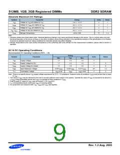
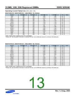
Absolute Maximum DC Ratings
Symbol
Parameter
Rating
Units
V
Notes
Voltage on V pin relative to V
V
- 1.0 V ~ 2.3 V
- 0.5 V ~ 2.3 V
- 0.5 V ~ 2.3 V
- 0.5 V ~ 2.3 V
-55 to +100
1
1
DD
SS
DD
Voltage on V
Voltage on V
pin relative to V
V
V
DDQ
DDL
SS
DDQ
pin relative to V
V
V
1
SS
DDL
Voltage on any pin relative to V
Storage Temperature
V
V
V
1
SS
IN, OUT
T
°C
1, 2
STG
Note :
1. Stresses greater than those listed under “Absolute Maximum Ratings” may cause permanent damage to the device. This is a stress rating only and
functional operation of the device at these or any other conditions above those indicated in the operational sections of this specification is not implied.
Exposure to absolute maximum rating conditions for extended periods may affect reliability.
2. Storage Temperature is the case surface temperature on the center/top side of the DRAM. For the measurement conditions, please refer to JESD51-2
standard.
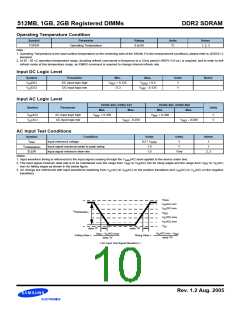
AC & DC Operating Conditions
Recommended DC Operating Conditions (SSTL - 1.8)
Rating
Symbol
Parameter
Units
Notes
Min.
1.7
Typ.
1.8
Max.
1.9
V
Supply Voltage
V
V
DD
V
Supply Voltage for DLL
Supply Voltage for Output
Input Reference Voltage
Termination Voltage
1.7
1.8
1.9
4
4
DDL
V
1.7
1.8
1.9
V
DDQ
V
0.49*V
0.50*V
0.51*V
DDQ
mV
V
1,2
3
REF
DDQ
DDQ
V
V
-0.04
V
V
+0.04
REF
TT
REF
REF
Note : There is no specific device V supply voltage requirement for SSTL-1.8 compliance. However under all conditions V
must be less than or equal
DDQ
DD
to V
.
DD
1. The value of V
may be selected by the user to provide optimum noise margin in the system. Typically the value of V
is expected to be about 0.5
REF
REF
x V
of the transmitting device and V
is expected to track variations in V
.
DDQ
DDQ
REF
2. Peak to peak AC noise on V
may not exceed +/-2% V
(DC).
REF
REF
3. V of transmitting device must track V
of receiving device.
REF
TT
4. AC parameters are measured with V , V
and V
tied together.
DDL
DD
DDQ
Rev. 1.2 Aug. 2005

 SAMSUNG [ SAMSUNG ]