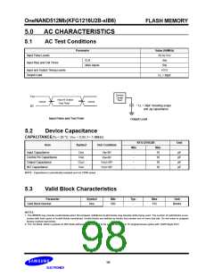
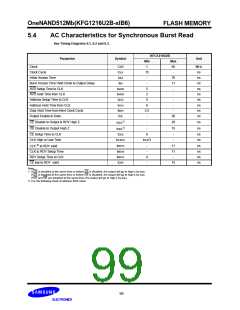
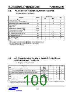
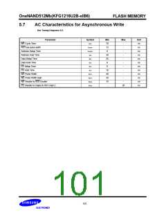
OneNAND512Mb(KFG1216U2B-xIB6)
FLASH MEMORY
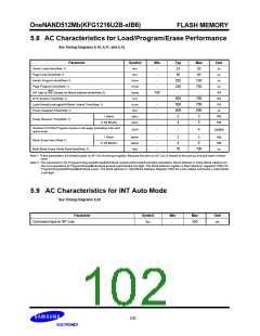
5.8 AC Characteristics for Load/Program/Erase Performance
See Timing Diagrams 6.10, 6.11, and 6.12
Parameter
Symbol
tRD1
Min
Typ
23
Max
35
Unit
µs
Sector Load time(Note 1)
Page Load time(Note 1)
-
tRD2
µs
-
30
45
Sector Program time(Note 1)
tPGM1
tPGM2
-
205
220
-
720
750
-
µs
Page Program time(Note 1)
µs
-
t
INT high to WE Disable for Block address write(Note 2)
OTP Access Time(Note 1)
120
ns
ns
ns
µs
INTW
tOTP
tLOCK
tESP
-
-
-
-
500
500
400
2
700
700
500
3
Lock/Unlock/Lock-tight/All Block Unlock Time(Note 1)
Erase Suspend Time(Note 1)
1 Block
2~64 Blocks
tERS1
tERS2
ms
ms
Erase Resume Time(Note 1)
4
6
Number of Partial Program Cycles in the page (Including main and
spare area)
NOP
-
-
4
cycles
1 Block
Block Erase time (Note 1)
tBERS1
tBERS2
tRD3
-
-
-
2
4
3
6
ms
ms
µs
2~64 Blocks
Multi Block Erase Verify Read time(Note 1)
70
100
Note1. These parameters are tested based on INT bit of interrupt register. Because the time on INT pin is related to the pull-up and pull-down resistor
value.
Note 2. This parameter is for Program/Copy-back/Erase/Multi-block erase/Lock/Unlock/Lock-tight operations. Block address is Flash Block address for
the next operations of Program/Erase/Multi-block erase/Lock/Unlock/Lock-tight. The block address register is Start address1 register(F100h) for
Program/Copyback/Erase/Multi-block erase. The block address is Start Block Address Register F24C for Lock related command- Lock/Unlock/
Lock-tight.
5.9 AC Characteristics for INT Auto Mode
See Timing Diagrams 6.20
Parameter
Command Input to INT Low
Symbol
Min
Max
Unit
-
200
ns
tWB
102

 SAMSUNG [ SAMSUNG ]