OneNAND512Mb(KFG1216U2B-xIB6)
FLASH MEMORY
3.7.2.1 Continuous Linear Burst Read Operation
See Timing Diagram 6.2
First Clock Cycle
The initial word is output at tIAA after the rising edge of the first CLK cycle. The RDY output indicates the initial word is ready to the
system by pulsing high. If the device is accessed synchronously while it is set to Asynchronous Read Mode, the first data can still be
read out.
Subsequent Clock Cycles
Subsequent words are output (Burst Access Time from Valid Clock to Output) tBA after the rising edge of each successive clock
cycle, which automatically increments the internal address counter.
Terminating Burst Read
The device will continue to output sequential burst data until the system asserts CE high, or RP low, wrapping around until it reaches
the designated address (see Section 2.7.3 for address map information). Alternately, a Cold/Warm/Hot Reset, or a WE low pulse will
terminate the burst read operation.
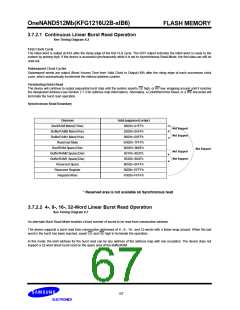
Synchronous Read Boundary
Division
Add.map(word order)
0000h~01FFh
0200h~05FFh
0600h~09FFh
0A00h~7FFFh
8000H~800Fh
8010h~802Fh
8030h~804Fh
8050h~8FFFh
9000h~EFFFh
F000h~FFFFh
BootRAM Main(0.5Kw)
BufferRAM0 Main(1Kw)
BufferRAM1 Main(1Kw)
Reserved Main
Not Support
Not Support
BootRAM Spare(16w)
BufferRAM0 Spare(32w)
BufferRAM1 Spare(32w)
Reserved Spare
Not Support
Not Support
Not Support
Reserved Register
Register(4Kw)
* Reserved area is not available on Synchronous read
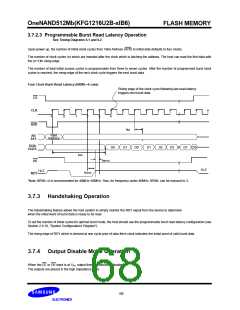
3.7.2.2 4-, 8-, 16-, 32-Word Linear Burst Read Operation
See Timing Diagram 6.1
An alternate Burst Read Mode enables a fixed number of words to be read from consecutive address.
The device supports a burst read from consecutive addresses of 4-, 8-, 16-, and 32-words with a linear-wrap around. When the last
word in the burst has been reached, assert CE and OE high to terminate the operation.
In this mode, the start address for the burst read can be any address of the address map with one exception. The device does not
support a 32-word linear burst read on the spare area of the BufferRAM.
67

 SAMSUNG [ SAMSUNG ]