OneNAND512Mb(KFG1216U2B-xIB6)
FLASH MEMORY
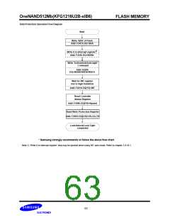
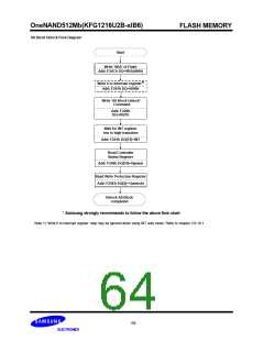
All Block Unlock Flow Diagram
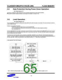
Start
Write ’SBA’ of Flash
Add: F24Ch DQ=SBA(000h)
Write 0 to interrupt register1)
Add: F241h DQ=0000h
Write ’All Block Unlock’
Command
Add: F220h
DQ=0027h
Wait for INT register
low to high transition
Add: F241h DQ[15]=INT
Read Controller
Status Register
Add: F240h DQ[10]=0(pass)
Read Write Protection Register
Add: F24Eh DQ[2]=1(unlock)
Unlock All Block
completed
* Samsung strongly recommends to follow the above flow chart
Note 1) ’Write 0 to interrupt register’ step may be ignored when using INT auto mode. Refer to chapter 2.8.18.1
64

 SAMSUNG [ SAMSUNG ]