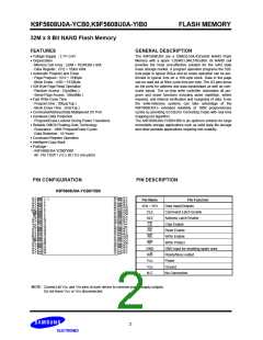
K9F5608U0A-YCB0,K9F5608U0A-YIB0
FLASH MEMORY
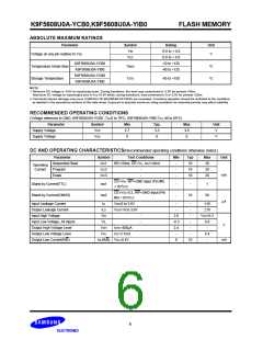
ABSOLUTE MAXIMUM RATINGS
Parameter
Symbol
VIN
Rating
Unit
-0.6 to + 4.6
-0.6 to + 4.6
-10 to +125
-40 to +125
Voltage on any pin relative to VSS
V
VCC
K9F5608U0A-YCB0
Temperature Under Bias
TBIAS
TSTG
°C
°C
K9F5608U0A-YIB0
K9F5608U0A-YCB0
K9F5608U0A-YIB0
Storage Temperature
-65 to +150
NOTE :
1. Minimum DC voltage is -0.6V on input/output pins. During transitions, this level may undershoot to -2.0V for periods <30ns.
Maximum DC voltage on input/output pins is VCC,+0.3V which, during transitions, may overshoot to VCC+2.0V for periods <20ns.
2. Permanent device damage may occur if ABSOLUTE MAXIMUM RATINGS are exceeded. Functional operation should be restricted to the conditions
as detailed in the operational sections of this data sheet. Exposure to absolute maximum rating conditions for extended periods may affect reliability.
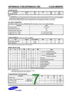
RECOMMENDED OPERATING CONDITIONS
(Voltage reference to GND, K9F5608U0A-YCB0 :TA=0 to 70°C, K9F5608U0A-YIB0:TA=-40 to 85°C)
Parameter
Supply Voltage
Supply Voltage
Symbol
VCC
Min
2.7
0
Typ.
3.3
0
Max
3.6
0
Unit
V
VSS
V
DC AND OPERATING CHARACTERISTICS(Recommended operating conditions otherwise noted.)
Parameter
Sequential Read
Program
Symbol
Test Conditions
Min
Typ
Max
Unit
ICC1
tRC=50ns, CE=VIL, IOUT=0mA
-
-
-
10
20
Operating
Current
ICC2
-
-
10
20
mA
Erase
ICC3
10
20
CE=VIH, WP=GND input (Pin #6)
= 0V/VCC
Stand-by Current(TTL)
ISB1
ISB2
-
-
-
1
CE=VCC-0.2, WP=GND input (Pin
#6) = 0V/VCC
Stand-by Current(CMOS)
10
50
mA
Input Leakage Current
Output Leakage Current
Input High Voltage
ILI
ILO
VIN=0 to 3.6V
-
-
-
-
±10
VOUT=0 to 3.6V
±10
VIH
VIL
-
-
2.0
-0.3
2.4
-
-
VCC+0.3
Input Low Voltage, All inputs
Output High Voltage Level
Output Low Voltage Level
Output Low Current(R/B)
-
0.8
-
V
VOH
VOL
IOH=-400mA
IOL=2.1mA
-
-
0.4
-
IOL(R/B) VOL=0.4V
8
10
mA
6

 SAMSUNG [ SAMSUNG ]