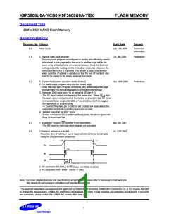
K9F5608U0A-YCB0,K9F5608U0A-YIB0
FLASH MEMORY
32M x 8 Bit NAND Flash Memory
FEATURES
GENERAL DESCRIPTION
· Voltage Supply : 2.7V~3.6V
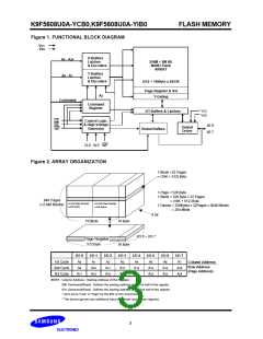
The K9F5608U0A are a 32M(33,554,432)x8bit NAND Flash
Memory with a spare 1,024K(1,048,576)x8bit. Its NAND cell
provides the most cost-effective solution for the solid state
mass storage market. A program operation programs the 528-
byte page in typical 200ms and an erase operation can be per-
formed in typical 2ms on a 16K-byte block. Data in the page
can be read out at 50ns cycle time per byte. The I/O pins serve
as the ports for address and data input/output as well as com-
mand inputs. The on-chip write controller automates all pro-
gram and erase functions including pulse repetition, where
required, and internal verification and margining of data. Even
the write-intensive systems can take advantage of the
K9F5608U0A¢s extended reliability of 100K program/erase
cycles by providing ECC(Error Correcting Code) with real time
mapping-out algorithm.
· Organization
- Memory Cell Array : (32M + 1024K)bit x 8bit
- Data Register : (512 + 16)bit x8bit
· Automatic Program and Erase
- Page Program : (512 + 16)Byte
- Block Erase : (16K + 512)Byte
· 528-Byte Page Read Operation
- Random Access : 10ms(Max.)
- Serial Page Access : 50ns(Min.)
· Fast Write Cycle Time
- Program time : 200ms(Typ.)
- Block Erase Time : 2ms(Typ.)
· Command/Address/Data Multiplexed I/O Port
· Hardware Data Protection
- Program/Erase Lockout During Power Transitions
· Reliable CMOS Floating-Gate Technology
- Endurance : 100K Program/Erase Cycles
- Data Retention : 10 Years
The K9F5608U0A-YCB0/YIB0 is an optimum solution for large
nonvolatile storage applications such as solid state file storage
and other portable applications requiring non-volatility.
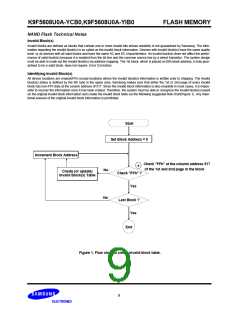
· Command Register Operation
· Intelligent Copy-Back
· Package :
- K9F5608U0A-YCB0/YIB0 :
48 - Pin TSOP I (12 x 20 / 0.5 mm pitch)
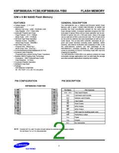
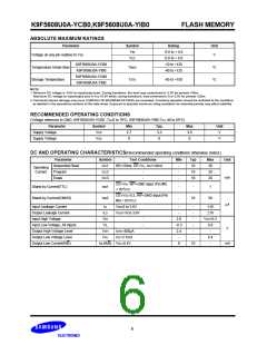
PIN CONFIGURATION
PIN DESCRIPTION
K9F5608U0A-YCB0/YIB0
N.C
N.C
N.C
N.C
I/O7
I/O6
I/O5
I/O4
N.C
N.C
N.C
Vcc
Vss
N.C
N.C
N.C
I/O3
I/O2
I/O1
I/O0
N.C
N.C
N.C
N.C
N.C
N.C
N.C
N.C
N.C
GND
R/B
RE
48
47
46
45
44
43
42
41
40
39
38
37
36
35
34
33
32
31
30
29
28
27
26
25
1
2
Pin Name
I/O0 ~ I/O7
CLE
Pin Function
Data Input/Outputs
3
4
5
6
Command Latch Enable
Address Latch Enable
Chip Enable
7
8
CE
9
ALE
N.C
N.C
Vcc
Vss
N.C
N.C
CLE
ALE
WE
WP
N.C
N.C
N.C
N.C
N.C
10
11
12
13
14
15
16
17
18
19
20
21
22
23
24
CE
RE
Read Enable
WE
Write Enable
WP
Write Protect
GND
R/B
GND input for enabling spare area
Ready/Busy output
Power
VCC
VSS
Ground
N.C
No Connection
NOTE : Connect all VCC and VSS pins of each device to common power supply outputs.
Do not leave VCC or VSS disconnected.
2

 SAMSUNG [ SAMSUNG ]