K9F5608U0A-YCB0,K9F5608U0A-YIB0
FLASH MEMORY
PRODUCT INTRODUCTION
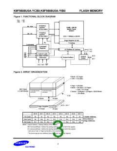
The K9F5608U0A is a 264Mbit(276,824,064 bit) memory organized as 65,536 rows(pages) by 528 columns. Spare sixteen columns
are located from column address of 512 to 527. A 528-byte data register is connected to memory cell arrays accommodating data
transfer between the I/O buffers and memory during page read and page program operations. The memory array is made up of 16
cells that are serially connected to form a NAND structure. Each of the 16 cells resides in a different page. A block consists of the 32
pages formed by two NAND structures, totaling 8448 NAND structures of 16 cells. The array organization is shown in Figure 2. The
program and read operations are executed on a page basis, while the erase operation is executed on a block basis. The memory
array consists of 2048 separately erasable 16K-byte blocks. It indicates that the bit by bit erase operation is prohibited on the
K9F5608U0A.
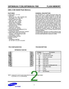
The K9F5608U0A has addresses multiplexed into 8 I/O¢s. This scheme dramatically reduces pin counts and allows systems upgrades
to future densities by maintaining consistency in system board design. Command, address and data are all written through I/O¢s by
bringing WE to low while CE is low. Data is latched on the rising edge of WE. Command Latch Enable(CLE) and Address Latch
Enable(ALE) are used to multiplex command and address respectively, via the I/O pins. All commands require one bus cycle except
for Block Erase command which requires two cycles: one cycle for erase-setup and another for erase-execution after block address
loading. The 32M byte physical space requires 25 addresses, thereby requiring three cycles for byte-level addressing: column
address, low row address and high row address, in that order. Page Read and Page Program need the same three address cycles fol-
lowing the required command input. In Block Erase operation, however, only the two row address cycles are used. Device operations
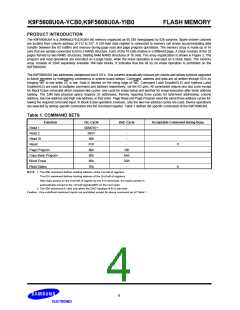
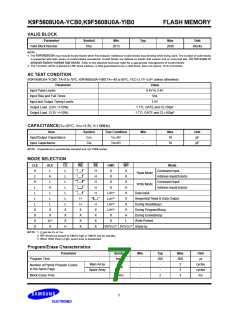
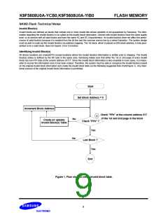
are selected by writing specific commands into the command register. Table 1 defines the specific commands of the K9F5608U0A.
Table 1. COMMAND SETS
Function
1st. Cycle
00h/01h(1)
50h(2)
90h
2nd. Cycle
Acceptable Command during Busy
Read 1
Read 2
Read ID
Reset
-
-
-
FFh
-
O
O
Page Program
Copy-Back Program
Block Erase
80h
10h
8Ah
D0h
-
00h
60h
Read Status
70h
NOTE : 1. The 00h command defines starting address of the 1st half of registers.
The 01h command defines starting address of the 2nd half of registers.
After data access on the 2nd half of register by the 01h command, the status pointer is
automatically moved to the 1st half register(00h) on the next cycle.
2. The 50h command is valid only when the GND input(pin # 6) is low level.
Caution : Any undefined command inputs are prohibited except for above command set of Table 1.
4

 SAMSUNG [ SAMSUNG ]