K9F5608U0A-YCB0,K9F5608U0A-YIB0
FLASH MEMORY
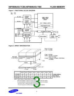
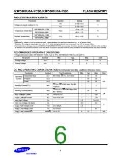
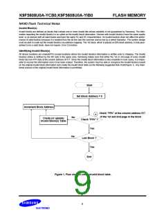
Figure 1. FUNCTIONAL BLOCK DIAGRAM
VCC
VSS
X-Buffers
A9 - A24
Latches
256M + 8M Bit
NAND Flash
ARRAY
& Decoders
Y-Buffers
A0 - A7
Latches
& Decoders
(512 + 16)Byte x 65536
Page Register & S/A
Y-Gating
A8
Command
Command
Register
VCC
VSS
I/O Buffers & Latches
Global Buffers
CE
RE
WE
Control Logic
& High Voltage
Generator
I/0 0
Output
Driver
I/0 7
CLE ALE
WP
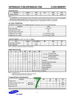
Figure 2. ARRAY ORGANIZATION
1 Block =32 Pages
= (16K + 512) Byte
1 Page = 528 Byte
1 Block = 528 Byte x 32 Pages
= (16K + 512) Byte
1 Device = 528Bytes x 32Pages x 2048 Blocks
= 264 Mbits
64K Pages
(=2,048 Blocks)
1st half Page Register
(=256 Bytes)
2nd half Page Register
(=256 Bytes)
8 bit
512Byte
16 Byte
16 Byte
I/O 0 ~ I/O 7
Page Register
512 Byte
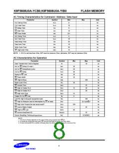
I/O 0
A0
I/O 1
A1
I/O 2
I/O 3
A3
I/O 4
A4
I/O 5
A5
I/O 6
A6
I/O 7
A7
1st Cycle
A2
Column Address
Row Address
(Page Address)
2nd Cycle
3rd Cycle
A9
A10
A18
A11
A19
A12
A20
A13
A21
A14
A22
A15
A23
A16
A24
A17
NOTE : Column Address : Starting Address of the Register.
00h Command(Read) : Defines the starting address of the 1st half of the register.
01h Command(Read) : Defines the starting address of the 2nd half of the register.
* A8 is set to "Low" or "High" by the 00h or 01h Command.
* The device ignores any additional input of address cycles than reguired.
3

 SAMSUNG [ SAMSUNG ]