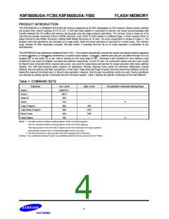
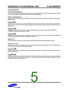
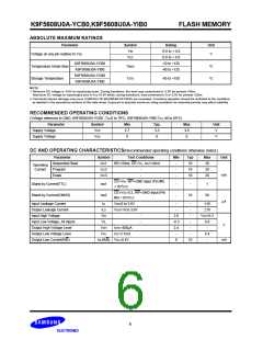
K9F5608U0A-YCB0,K9F5608U0A-YIB0
FLASH MEMORY
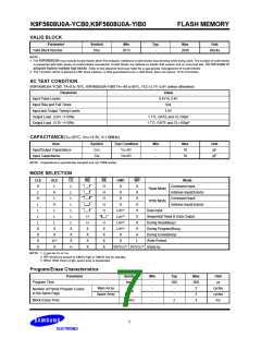
AC Timing Characteristics for Command / Address / Data Input
Parameter
Symbol
tCLS
tCLH
tCS
Min
Max
Unit
ns
ns
ns
ns
ns
ns
ns
ns
ns
ns
ns
CLE Set-up Time
CLE Hold Time
CE Setup Time
CE Hold Time
0
-
-
-
-
-
-
-
-
-
-
-
10
0
tCH
10
25(1)
0
WE Pulse Width
ALE Setup Time
ALE Hold Time
Data Setup Time
Data Hold Time
Write Cycle Time
tWP
tALS
tALH
tDS
10
20
10
50
15
tDH
tWC
WE High Hold Time
tWH
NOTE : 1. If tCS is set less than 10ns, tWP must be minimum 35ns, otherwise, tWP may be minimum 25ns.
AC Characteristics for Operation
Parameter
Data Transfer from Cell to Register
ALE to RE Delay( ID read )
ALE to RE Delay(Read cycle)
CLE to RE Delay
Symbol
tR
Min
-
Max
Unit
10
ms
ns
ns
ns
ns
ns
ns
ns
ns
ns
ns
ns
ns
ns
ns
ns
ns
ns
ns
ms
tAR1
tAR2
tCLR
tRR
20
50
50
20
30
-
-
-
-
Ready to RE Low
-
RE Pulse Width
tRP
-
WE High to Busy
tWB
100
Read Cycle Time
tRC
50
-
-
RE Access Time
tREA
tRHZ
tCHZ
tREH
tIR
35
RE High to Output Hi-Z
15
-
30
CE High to Output Hi-Z
20
RE High Hold Time
15
0
-
Output Hi-Z to RE Low
-
Last RE High to Busy(at sequential read)
CE High to Ready(in case of interception by CE at read)
CE High Hold Time(at the last serial read)(2)
CE Low to Status Output
WE High to RE Low
tRB
-
100
50 +tr(R/B)(1)
tCRY
tCEH
tCEA
tWHR
tREADID
tRST
-
100
-
-
45
60
-
-
RE access time(Read ID)
Device Resetting Time(Read/Program/Erase)
35
5/10/500(3)
-
NOTE :
1. The time to Ready depends on the value of the pull-up resistor tied R/B pin.
2. To break the sequential read cycle, CE must be held high for longer time than tCEH.
3. If reset command(FFh) is written at Ready state, the device goes into Busy for maximum 5us.
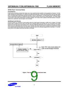
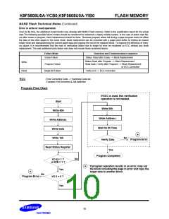
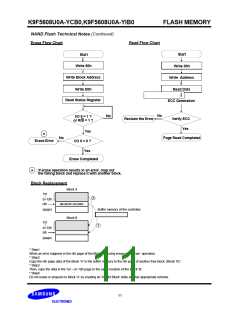
8

 SAMSUNG [ SAMSUNG ]