K9F5608U0A-YCB0,K9F5608U0A-YIB0
FLASH MEMORY
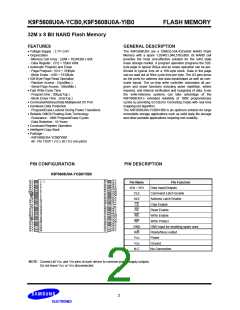
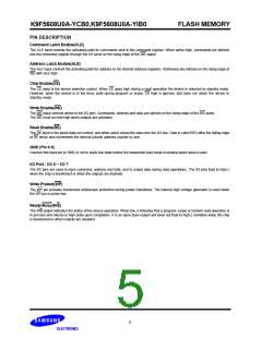
PIN DESCRIPTION
Command Latch Enable(CLE)
The CLE input controls the activating path for commands sent to the command register. When active high, commands are latched
into the command register through the I/O ports on the rising edge of the WE signal.
Address Latch Enable(ALE)
The ALE input controls the activating path for address to the internal address registers. Addresses are latched on the rising edge of
WE with ALE high.
Chip Enable(CE)
The CE input is the device selection control. When CE goes high during a read operation the device is returned to standby mode.
However, when the device is in the Busy state during program or erase, CE high is ignored, and does not return the device to
standby mode.
Write Enable(WE)
The WE input controls writes to the I/O port. Commands, address and data are latched on the rising edge of the WE pulse.
The WE must be held high when outputs are activated.
Read Enable(RE)
The RE input is the serial data-out control, and when active drives the data onto the I/O bus. Data is valid tREA after the falling edge
of RE which also increments the internal column address counter by one.
GND (Pin # 6)
Connect this input pin to GND or set to static low state unless the sequential read mode excluding spare area is used.
I/O Port : I/O 0 ~ I/O 7
The I/O pins are used to input command, address and data, and to output data during read operations. The I/O pins float to high-z
when the chip is deselected or when the outputs are disabled.
Write Protect(WP)
The WP pin provides inadvertent write/erase protection during power transitions. The internal high voltage generator is reset when
the WP pin is active low.
Ready/Busy(R/B)
The R/B output indicates the status of the device operation. When low, it indicates that a program, erase or random read operation is
in process and returns to high state upon completion. It is an open drain output and does not float to high-z condition when the chip
is deselected or when outputs are disabled.
5

 SAMSUNG [ SAMSUNG ]