K9F5608U0A-YCB0,K9F5608U0A-YIB0
FLASH MEMORY
READ STATUS
The device contains a Status Register which may be read to find out whether program or erase operation is completed, and whether
the program or erase operation is completed successfully. After writing 70h command to the command register, a read cycle outputs
the content of the Status Register to the I/O pins on the falling edge of CE or RE, whichever occurs last. This two line control allows
the system to poll the progress of each device in multiple memory connections even when R/B pins are common-wired. RE or CE
does not need to be toggled for updated status. Refer to table 2 for specific Status Register definitions. The command register
remains in Status Read mode until further commands are issued to it. Therefore, if the status register is read during a random read
cycle, a read command(00h or 50h) should be given before sequential page read cycle.
Table2. Read Status Register Definition
I/O #
Status
Definition
"0" : Successful Program / Erase
I/O 0
Program / Erase
"1" : Error in Program / Erase
I/O 1
I/O 2
I/O 3
I/O 4
I/O 5
I/O 6
I/O 7
"0"
"0"
"0"
"0"
"0"
Reserved for Future
Use
Device Operation
Write Protect
"0" : Busy
"1" : Ready
"1" : Not Protected
"0" : Protected
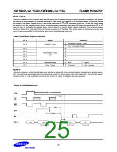
READ ID
The device contains a product identification mode, initiated by writing 90h to the command register, followed by an address input of
00h. Two read cycles sequentially output the manufacture code(ECh), and the device code (75h) respectively. The command register
remains in Read ID mode until further commands are issued to it. Figure 10 shows the operation sequence.
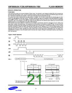
Figure 10. Read ID Operation
tCLR
CLE
tCEA
CE
WE
tAR1
ALE
tWHR
RE
tREA
I/O0~7
00h
75h
90h
ECh
Address. 1cycle
Maker code
Device code
25

 SAMSUNG [ SAMSUNG ]