K9F5608U0A-YCB0,K9F5608U0A-YIB0
FLASH MEMORY
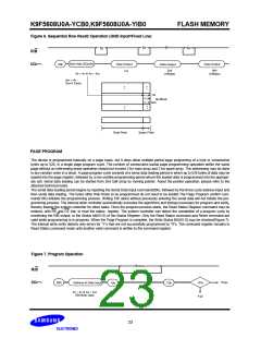
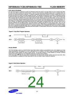
COPY-BACK PROGRAM
The copy-back program is configured to quickly and efficiently rewrite data stored in one page within the array to another page within
the same array without utilizing an external memory. Since the time-consuming sequently-reading and its re-loading cycles are
removed, the system performance is improved. The benefit is especially obvious when a portion of a block is updated and the rest of
the block also need to be copied to the newly assigned free block. The operation for performing a copy-back is a sequential execution
of page-read without burst-reading cycle and copying-program with the address of destination page. A normal read operation with
"00h" command with the address of the source page moves the whole 528byte data into the internal buffer. As soon as the Flash
returns to Ready state, copy-back programming command "8Ah" may be given with three address cycles of target page followed. The
data stored in the internal buffer is then programmed directly into the memory cells of the destination page. Once the Copy-Back Pro-
gram is finished, any additional partial page programming into the copied pages is prohibited before erase. Since the memory array is
internally partitioned into two different planes, copy-back program is allowed only within the same memory plane. Thus, A14, the
plane address, of source and destination page address must be the same. "When there is a program-failure at Copy-Back opera-
tion, error is reported by pass/fail status. But, if Copy-Back operations are accumulated over time, bit error due to charge
loss is not checked by external error detection/correction scheme. For this reason, two bit error correction is recommended
for the use of Copy-Back operation."
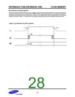
Figure 8. Copy-Back Program Operation
tR
tPROG
R/B
Add.(3Cycles)
Pass
I/O0~7
00h
Add.(3Cycles)
I/O0
Fail
8Ah
70h
A0 ~ A7 & A9 ~ A24
Source Address
A0 ~ A7 & A9 ~ A24
Destination Address
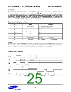
BLOCK ERASE
The Erase operation is done on a block(16K Byte) basis. Block address loading is accomplished in two cycles initiated by an Erase
Setup command(60h). Only address A14 to A24 is valid while A9 to A13 is ignored. The Erase Confirm command(D0h) following the
block address loading initiates the internal erasing process. This two-step sequence of setup followed by execution command
ensures that memory contents are not accidentally erased due to external noise conditions.
At the rising edge of WE after the erase confirm command input, the internal write controller handles erase and erase-verify. When
the erase operation is completed, the Write Status Bit(I/O 0) may be checked. Figure 8 details the sequence.
Figure 9. Block Erase Operation
tBERS
R/B
Pass
I/O0~7
60h
I/O0
Fail
70h
Address Input(2Cycle)
Block Add. : A9 ~ A24
D0h
24

 SAMSUNG [ SAMSUNG ]