K9F5608U0A-YCB0,K9F5608U0A-YIB0
FLASH MEMORY
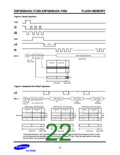
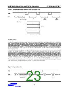
Figure 6. Sequential Row Read2 Operation (GND Input=Fixed Low)
tR
tR
tR
R/B
Start Add.(3Cycle)
Data Output
1st
Data Output
I/O0~7
50h
Data Output
2nd
(16Byte)
Nth
(16Byte)
A0 ~ A3 & A9 ~ A24
(A4 ~ A7 :
Don¢t Care)
1st
Block
Nth
Data Field
Spare Field
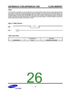
PAGE PROGRAM
The device is programmed basically on a page basis, but it does allow multiple partial page programing of a byte or consecutive
bytes up to 528, in a single page program cycle. The number of consecutive partial page programming operation within the same
page without an intervening erase operation should not exceed 2 for main array and 3 for spare array. The addressing may be done
in any random order in a block. A page program cycle consists of a serial data loading period in which up to 528 bytes of data may be
loaded into the page register, followed by a non-volatile programming period where the loaded data is programmed into the appropri-
ate cell. Serial data loading can be started from 2nd half array by moving pointer. About the pointer operation, please refer to the
attached technical notes.
The serial data loading period begins by inputting the Serial Data Input command(80h), followed by the three cycle address input and
then serial data loading. The bytes other than those to be programmed do not need to be loaded.The Page Program confirm com-
mand(10h) initiates the programming process. Writing 10h alone without previously entering the serial data will not initiate the pro-
gramming process. The internal write controller automatically executes the algorithms and timings necessary for program and verify,
thereby freeing the system controller for other tasks. Once the program process starts, the Read Status Register command may be
entered, with RE and CE low, to read the status register. The system controller can detect the completion of a program cycle by
monitoring the R/B output, or the Status bit(I/O 6) of the Status Register. Only the Read Status command and Reset command are
valid while programming is in progress. When the Page Program is complete, the Write Status Bit(I/O 0) may be checked(Figure 7).
The internal write verify detects only errors for "1"s that are not successfully programmed to "0"s. The command register remains in
Read Status command mode until another valid command is written to the command register.
Figure 7. Program Operation
tPROG
R/B
Pass
I/O0~7
80h
Address & Data Input
I/O0
Fail
10h
70h
A0 ~ A7 & A9 ~ A24
528 Byte Data
23

 SAMSUNG [ SAMSUNG ]