K7I163682B
K7I161882B
512Kx36 & 1Mx18 DDRII CIO b2 SRAM
512Kx36-bit, 1Mx18-bit DDRII CIO b2 SRAM
FEATURES
• 1.8V+0.1V/-0.1V Power Supply.
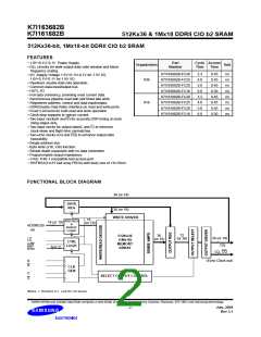
Part
Cycle Access
Organization
Unit
• DLL circuitry for wide output data valid window and future
freguency scaling.
Number
Time
Time
K7I163682B-FC30
K7I163682B-FC25
K7I163682B-FC20
K7I163682B-FC16
K7I161882B-FC30
K7I161882B-FC25
K7I161882B-FC20
K7I161882B-FC16
3.3
4.0
5.0
6.0
3.3
4.0
5.0
6.0
0.45
0.45
0.45
0.50
0.45
0.45
0.45
0.50
ns
ns
ns
ns
ns
ns
ns
ns
• I/O Supply Voltage 1.5V+0.1V/-0.1V for 1.5V I/O,
1.8V+0.1V/-0.1V for 1.8V I/O.
X36
X18
• Pipelined, double-data rate operation.
• Common data input/output bus .
• HSTL I/O
• Full data coherency, providing most current data.
• Synchronous pipeline read with self timed late write.
• Registered address, control and data input/output.
• DDR(Double Data Rate) Interface on read and write ports.
• Fixed 2-bit burst for both read and write operation.
• Clock-stop supports to reduce current.
• Two input clocks(K and K) for accurate DDR timing at clock
rising edges only.
• Two input clocks for output data(C and C) to minimize
clock-skew and flight-time mismatches.
• Two echo clocks (CQ and CQ) to enhance output data
traceability.
• Single address bus.
• Byte write (x18, x36) function.
• Simple depth expansion with no data contention.
• Programmable output impedance.
• JTAG 1149.1 compatible test access port.
• 165FBGA(11x15 ball array FBGA) with body size of 13x15mm
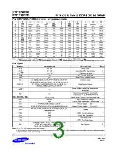
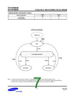
FUNCTIONAL BLOCK DIAGRAM
36 (or 18)
DATA
REG
36 (or 18)
WRITE DRIVER
18
ADD REG
&
18 (or 19)
4(or 2)
(or 19)
ADDRESS
A0
BURST
LOGIC
72
36
512Kx36
(1Mx18)
MEMORY
ARRAY
36 (or 18)
DQ
(or 36)
(or 18)
LD
R/W
BWX
CTRL
LOGIC
CQ, CQ
(Echo Clock out)
K
K
CLK
GEN
C
C
SELECT OUTPUT CONTROL
Notes: 1. Numbers in ( ) are for x18 device.
DDRII SRAM and Double Data Rate comprise a new family of products developed by Cypress, Renesas, IDT, NEC and Samsung technology.
July. 2004
Rev 3.1
- 2 -

 SAMSUNG [ SAMSUNG ]