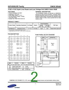
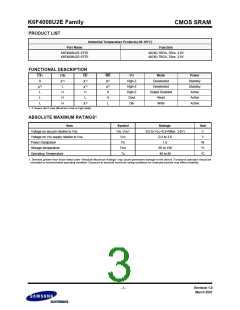
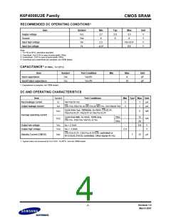
K6F4008U2E Family
CMOS SRAM
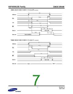
TIMING WAVEFORM OF WRITE CYCLE(3) (CS2 Controlled)
tWC
Address
CS1
tAS(3)
tCW(2)
tWR(4)
tAW
CS2
tCW(2)
tWP(1)
WE
tDH
tDW
Data in
Data Valid
High-Z
High-Z
Data out
NOTES (WRITE CYCLE)
1. A write occurs during the overlap of a low CS1, a high CS2 and a low WE. A write begins at the latest transition among CS1 goes low,
CS2 going high and WE going low: A write end at the earliest transition among CS1 going high, CS2 going low and WE going high, tWP
is measured from the begining of write to the end of write.
2. tCW is measured from the CS1 going low or CS2 going high to the end of write.
3. tAS is measured from the address valid to the beginning of write.
4. tWR is measured from the end of write to the address change. tWR1 applied in case a write ends as CS1 or WE going high tWR2 applied
in case a write ends as CS2 going to low.
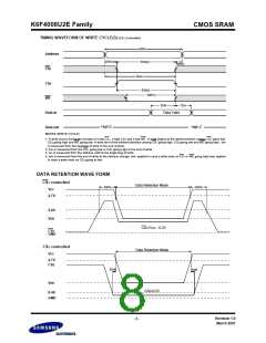
DATA RETENTION WAVE FORM
CS1 controlled
Data Retention Mode
tSDR
tRDR
VCC
2.7V
2.2V
VDR
CS1³ VCC - 0.2V
CS1
GND
CS2 controlled
Data Retention Mode
VCC
2.7V
CS2
tSDR
tRDR
VDR
CS2£0.2V
0.4V
GND
Revision 1.0
March 2001
- 8 -

 SAMSUNG [ SAMSUNG ]