K6F4008U2E Family
CMOS SRAM
512K x 8 bit Super Low Power and Low Voltage Full CMOS Static RAM
FEATURES
GENERAL DESCRIPTION
· Process Technology: Full CMOS
· Organization: 512K x8 bit
The K6F4008U2E families are fabricated by SAMSUNG¢s
advanced full CMOS process technology. The families support
industrial temperature range and Chip Scale Package for user
flexibility of system design. The families also supports low data
retention voltage for battery back-up operation with low data
retention current.
· Power Supply Voltage: 2.7~3.3V
· Low Data Retention Voltage: 1.5V(Min)
· Three State Outputs
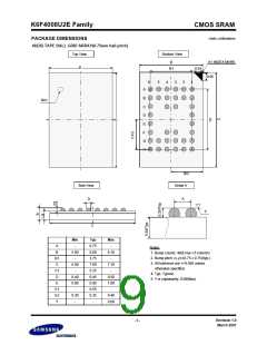
· Package Type: 48(36)-TBGA-6.00x7.00
PRODUCT FAMILY
Power Dissipation
Product Family Operating Temperature Vcc Range
Speed
PKG Type
Standby
(ISB1, Typ.)
Operating
(ICC1, Max)
551)/70ns
1.0mA2)
K6F4008U2E-F
Industrial(-40~85°C)
2.7~3.3V
2mA
48(36)-TBGA-6.00x7.00
1. The parameter is measured with 30pF test load.
2. Typical value are at VCC=3.0V, TA=25°C and not 100% tested.
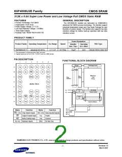
PIN DESCRIPTION
FUNCTIONAL BLOCK DIAGRAM
1
2
3
4
5
6
Clk gen.
Precharge circuit.
A
B
C
D
E
F
A0
A1
A2
CS2
WE
A3
A4
A5
A6
A7
A8
I/O5
I/O6
VSS
VCC
I/O7
I/O8
A9
I/O1
I/O2
VCC
VSS
I/O3
I/O4
A14
Memory
Cell
Array
Row
select
DNU
Row
Address
48(36)-TBGA
I/O1
I/O8
Data
cont
I/O Circuit
A18
CS1
A11
A17
A16
A12
Column select
G
H
OE
A10
A15
A13
Data
cont
Column Address
CS1
Name
Function
Name
Function
Control
logic
CS2
WE
OE
CS1, CS2 Chip Select Inputs
I/O1~I/O8 Data Inputs/Outputs
OE
Output Enable Input
Write Enable Input
Vcc
Vss
Power
WE
Ground
A0~A18 Address Inputs
DNU
Do Not Use
SAMSUNG ELECTRONICS CO., LTD. reserves the right to change products and specifications without notice.
Revision 1.0
March 2001
- 2 -

 SAMSUNG [ SAMSUNG ]