K6F4008U2E Family
CMOS SRAM
3)
VTM
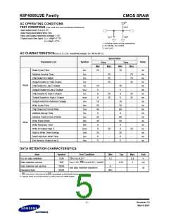
AC OPERATING CONDITIONS
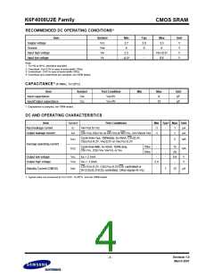
TEST CONDITIONS (Test Load and Test Input/Output Reference)
Input pulse level: 0.4 to 2.2V
2)
R1
Input rising and falling time: 5ns
Input and output reference voltage: 1.5V
Output load (See right): CL= 100pF+1TTL
CL=30pF+1TTL
1)
2)
CL
R2
1. Including scope and jig capacitance
2. R1=3070W, R2=3150W
3. VTM =2.8V
AC CHARACTERISTICS(Vcc=2.7~3.3V, Industrial product:TA=-40 to 85°C)
Speed Bins
Parameter List
Symbol
Units
55ns
70ns
Min
55
-
Max
Min
70
-
Max
Read Cycle Time
tRC
tAA
-
55
55
25
-
-
70
70
35
-
ns
ns
ns
ns
ns
ns
ns
ns
ns
ns
ns
ns
ns
ns
ns
ns
ns
ns
ns
Address Access Time
Chip Select to Output
tCO
tOE
tLZ
-
-
Output Enable to Valid Output
Chip Select to Low-Z Output
Output Enable to Low-Z Output
Chip Disable to High-Z Output
Output Disable to High-Z Output
Output Hold from Address Change
Write Cycle Time
-
-
Read
10
5
10
5
tOLZ
tHZ
-
-
0
20
20
-
0
25
25
-
tOHZ
tOH
tWC
tCW
tAS
0
0
10
55
45
0
10
70
60
0
-
-
Chip Select to End of Write
Address Set-up Time
-
-
-
-
Address Valid to End of Write
Write Pulse Width
tAW
tWP
tWR
tWHZ
tDW
tDH
45
40
0
-
60
50
0
-
-
-
Write
Write Recovery Time
-
-
Write to Output High-Z
0
20
-
0
20
-
Data to Write Time Overlap
Data Hold from Write Time
End Write to Output Low-Z
25
0
30
0
-
-
tOW
5
-
5
-
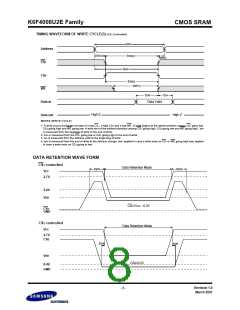
DATA RETENTION CHARACTERISTICS
Item
Vcc for data retention
Data retention current
Data retention set-up time
Recovery time
Symbol
VDR
Test Condition
Min
Typ
Max
Unit
V
CS1³ Vcc-0.2V1)
1.5
-
-
3.3
Vcc=1.5V, CS1³ Vcc-0.2V1), VIN³ 0V
0.52)
IDR
3
-
mA
tSDR
tRDR
0
-
-
See data retention waveform
ns
tRC
-
1. CS1³ Vcc-0.2V, CS2³ Vcc-0.2V(CS1 controlled) or 0£CS2£0.2V(CS2 controlled).
2. Typical value are measured at TA=25°C and not 100% tested.
Revision 1.0
March 2001
- 5 -

 SAMSUNG [ SAMSUNG ]