Preliminary
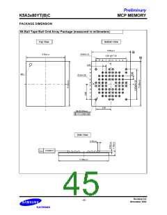
K5A3x80YT(B)C
MCP MEMORY
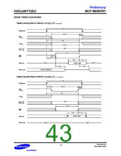
TIMING WAVEFORM OF WRITE CYCLE(3) (UB, LB Controlled)
tWC
Address
tCW(2)
tAW
tWR(4)
CS1
CS2
S
S
tCW(2)
tBW
UB, LB
WE
tAS(3)
tWP(1)
tDH
tDW
Data in
Data Valid
High-Z
Data out
High-Z
NOTES (WRITE CYCLE)
1. A write occurs during the overlap(tWP) of low CS1S and low WE. A write begins when CS1S goes low and WE goes low with asserting
UB or LB for single byte operation or simultaneously asserting UB and LB for double byte operation. A write ends at the earliest tran-
sition when CS1S goes high and WE goes high. The tWP is measured from the beginning of write to the end of write.
2. tCW is measured from the CS1S going low to the end of write.
3. tAS is measured from the address valid to the beginning of write.
4. tWR is measured from the end of write to the address change. tWR applied in case a write ends as CS1S or WE going high.
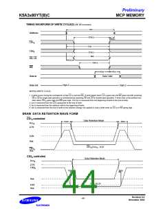
SRAM DATA RETENTION WAVE FORM
CS1S controlled
Data Retention Mode
tSDR
tRDR
Vcc
S
2.7V
2.2V
VDR
CS1 ³ Vcc - 0.2V
S
S
CS1
Vss
S
CS2S controlled
Data Retention Mode
Vcc
S
2.7V
CS2
S
tSDR
tRDR
VDR
CS2 £0.2V
S
0.4V
Vss
Revision 0.0
November 2002
- 44 -

 SAMSUNG [ SAMSUNG ]