Preliminary
K5A3x80YT(B)C
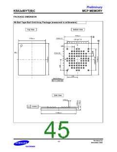
MCP MEMORY
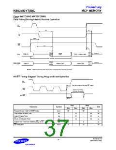
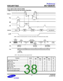
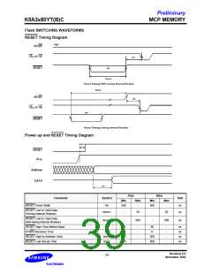
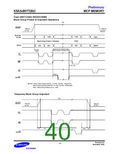
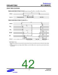
SRAM TIMING DIAGRAMS
TIMING WAVEFORM OF READ CYCLE(1) (Address Controlled, CS1S=OE=VIL, CS2S=WE=VIH, UB or/and LB=VIL)
tRC
Address
tAA
tOH
Data Valid
Data Out
Previous Data Valid
TIMING WAVEFORM OF READ CYCLE(2) (WE=VIH)
tRC
Address
tOH
tAA
tCO1
CS1
CS2
S
S
tCO2
tBA
tHZ
UB, LB
OE
tBHZ
tOHZ
tOE
tOLZ
tBLZ
tLZ
Data out
High-Z
Data Valid
NOTES (READ CYCLE)
1. tHZ and tOHZ are defined as the time at which the outputs achieve the open circuit conditions and are not referenced to output voltage
levels.
2. At any given temperature and voltage condition, tHZ(Max.) is less than tLZ(Min.) both for a given device and from device to device
interconnection.
Revision 0.0
November 2002
- 42 -

 SAMSUNG [ SAMSUNG ]