Preliminary
K5A3x80YT(B)C
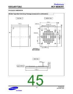
MCP MEMORY
SRAM AC CHARACTERISTICS
55ns
Units
Parameter List
Symbol
Min
Max
Read cycle time
tRC
tAA
55
-
-
55
55
25
55
-
ns
ns
ns
ns
ns
ns
ns
ns
ns
ns
ns
ns
ns
ns
ns
ns
ns
ns
ns
ns
ns
ns
ns
Address access time
Chip select to output
Output enable to valid output
UB, LB Access Time
tCO1, tCO2
tOE
-
-
tBA
-
Chip select to low-Z output
Read
tLZ1, tLZ2
tBLZ
10
10
5
UB, LB enable to low-Z output
Output enable to low-Z output
Chip disable to high-Z output
UB, LB disable to high-Z output
Output disable to high-Z output
Output hold from address change
Write cycle time
-
tOLZ
tHZ1, tHZ2
tBHZ
tOHZ
tOH
-
0
20
20
20
-
0
0
10
55
45
0
tWC
-
Chip select to end of write
Address set-up time
tCW
-
tAS
-
Address valid to end of write
UB, LB Valid to End of Write
tAW
45
45
40
0
-
tBW
-
Write
Write pulse width
tWP
-
Write recovery time
tWR
-
Write to output high-Z
Data to write time overlap
Data hold from write time
End write to output low-Z
tWHZ
tDW
0
20
-
20
0
tDH
-
tOW
5
-
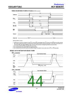
SRAM DATA RETENTION CHARACTERISTICS
Item
Symbol
VDR
Test Condition
CS1 ³ Vcc -0.2V
Min
1.5
-
Typ
Max
Unit
Vcc for data retention
-
0.5
-
3.3
15
-
V
S
S
S
Data retention current
Data retention set-up time
Recovery time
IDR
Vcc =3.0V, CS1 ³ Vcc -0.2V
mA
S
S
S
tSDR
0
See data retention waveform
ns
tRDR
tRC
-
-
1. CS1 ³ Vcc -0.2V, CS2 ³ Vcc -0.2V(CS1 controlled) or CS2 £0.2V(CS2 controlled)
S
S
S
S
S
S
S
2. Typical values are measured at Vcc=3.0V, Ta=25°C , not 100% tested.
Revision 0.0
November 2002
- 41 -

 SAMSUNG [ SAMSUNG ]