Preliminary
K5A3x80YT(B)C
MCP MEMORY
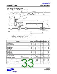
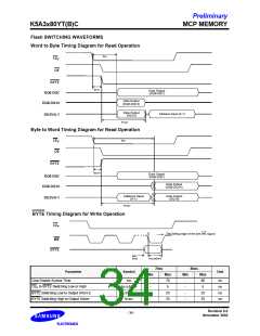
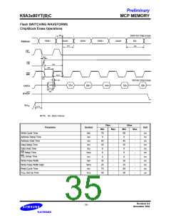
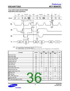
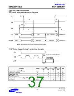
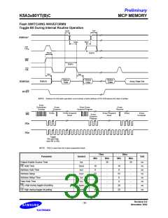
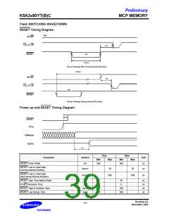
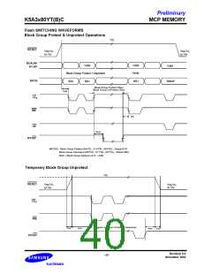
Flash SWITCHING WAVEFORMS
Data Polling During Internal Routine Operation
CE
F
tDF
tOE
OE
tOEH2
WE
tCE
tOH
HIGH-Z
Data In
Data In
DQ7
*DQ7 = Valid Data
DQ7
tPGM or tBERS
HIGH-Z
DQ0-DQ6
Valid Data
Status Data
NOTE: *DQ7=Vaild Data (The device has completed the internal operation).
RY/BY Timing Diagram During Program/Erase Operation
CE
F
The rising edge of the last WE signal
WE
Entire progrming
or erase operation
RY/BY
tBUSY
70ns
80ns
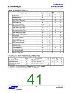
Parameter
Symbol
Unit
Min
Max
-
Min
Max
-
Program/Erase Valid to RY/BY Delay
Chip Enable Access Time
Output Enable Time
tBUSY
tCE
90
-
90
-
ns
ns
ns
ns
70
25
16
80
25
16
tOE
-
-
CE & OE Disable Time
tDF
-
-
F
Output Hold Time from Address, CE or OE
tOH
0
-
-
0
-
-
ns
ns
F
OE Hold Time
tOEH2
10
10
Revision 0.0
November 2002
- 37 -

 SAMSUNG [ SAMSUNG ]