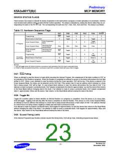
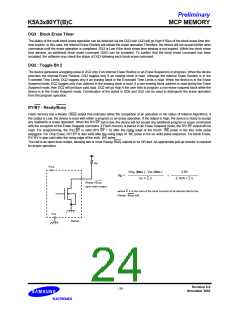
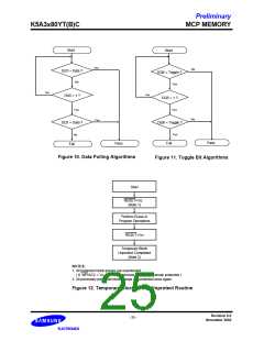
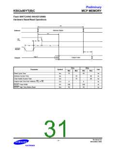
Preliminary
K5A3x80YT(B)C
MCP MEMORY
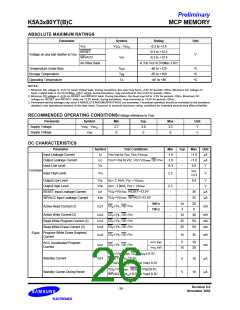
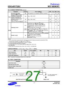
DC CHARACTERISTICS(Continued)
Parameter
Symbol
Test Conditions
Min Typ Max Unit
VIH=Vcc ±0.3V, VIL=VSS±0.3V, OE=VIL, IOL=IOH=0
Automatic Sleep Mode
ISB3
-
5
18
mA
F
Voltage for WP/ACC Block
Temporarily Unprotect and
Program Acceleration (4)
Vcc = 3.0V ± 0.3V
VHH
8.5
-
12.5
V
F
Flash
Voltage for Autoselect and
Block Protect (4)
Vcc = 3.0V ± 0.3V
VID
8.5
1.8
-
-
12.5
2.5
V
V
F
Low Vcc Lock-out Voltage (5)
VLKO
F
Cycle time=1ms, 100% duty, CS1 £0.2V,
S
CS2 ³ Vcc -0.2V, LB£0.2V and/or UB£0.2V
S
S
ICC1
ICC2
-
-
-
-
3
mA
mA
mA
All outputs open, VIN£0.2V or VIN³ Vcc -0.2V,
S
BYTE =Vcc ± 0.3V or Vss± 0.3V
Operating Current
Standby Current
S
S
Cycle time=Min, 100% duty, CS1 =VIL, CS2 =VIH,
S
S
LB=VIL and/or UB= VIL, All outputs open, VIN=VIL or
VIH, BYTE =Vcc ± 0.3V or Vss± 0.3V
SRAM
22
0.5
28
15
S
S
CS1 ³ Vcc -0.2V, CS2 ³ Vcc -0.2V (CS1 controlled)
S
S
S
S
S
or CS2 £0.2V (CS2 controlled),
S
S
ISB
BYTE =Vcc ± 0.3V or Vss± 0.3V,
S
S
Other input =0~Vcc
S
NOTES:
1. The ICC current listed includes both the DC operating current and the frequency dependent component(at 5 MHz).
The read current is typically 14 mA (@ VccF=3.0V , OE at VIH.)
2. ICC active during Internal Routine(program or erase) is in progress.
3. ICC active during Read while Write is in progress.
4. The high voltage ( VHH or VID ) must be used in the range of VccF = 3.0V ± 0.3V
5. Not 100% tested.
6. Typical values are measured at VccF = VccS = 3.0V, Ta=25°C , not 100% tested.
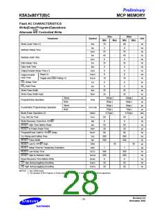
CAPACITANCE(TA = 25 °C, VccF = VccS = 3.3V, f = 1.0MHz)
Item
Symbol
CIN
Test Condition
VIN=0V
Min
Max
18
Unit
pF
Input Capacitance
-
-
-
Output Capacitance
Control Ball Capacitance
COUT
CIN2
VOUT=0V
VIN=0V
20
pF
18
pF
NOTE: Capacitance is periodically sampled and not 100% tested.
AC TEST CONDITION
Parameter
Value
0V to Vcc
5ns
Input Pulse Levels
Input Rise and Fall Times
Input and Output Timing Levels
Output Load
Vcc/2
CL = 30pF
Device
Vcc
Input & Output
Vcc/2
Vcc/2
* CL= 30pF including Scope
and Jig Capacitance
Test Point
CL
0V
Input Pulse and Test Point
Output Load
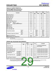
Revision 0.0
November 2002
- 27 -

 SAMSUNG [ SAMSUNG ]