K4S640832K
K4S641632K
Synchronous DRAM
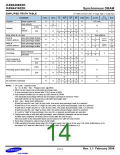
SIMPLIFIED TRUTH TABLE
(V=Valid, X=Don′t care, H=Logic high, L=Logic low)
A11,
CKEn-1 CKEn
CS
RAS
CAS
WE
DQM BA0,1
A10/AP
Note
Command
A9 ~ A0
Register
Refresh
Mode register set
Auto refresh
H
H
X
H
L
L
L
L
L
X
OP code
1,2
3
3
3
3
L
L
L
H
X
X
X
X
Entry
Self
refresh
L
H
L
H
X
L
H
X
H
H
X
H
Exit
L
H
H
H
X
X
Bank active & row addr.
Read &
column address
X
X
V
V
Row address
Auto precharge disable
Auto precharge enable
Auto precharge disable
Auto precharge enable
L
H
L
4
4,5
4
4,5
6
Column
address
L
H
L
H
Write &
column address
Column
address
H
H
H
X
X
X
L
L
L
H
H
L
L
H
H
L
L
L
X
X
X
V
H
Burst stop
Precharge
X
Bank selection
All banks
V
X
L
H
X
H
L
X
H
L
X
V
X
X
H
X
V
X
X
H
X
V
X
X
H
X
V
X
V
X
X
H
X
V
Entry
Exit
H
L
L
H
L
X
X
X
Clock suspend or
active power down
X
X
Entry
H
Precharge power down mode
H
L
Exit
L
H
H
H
X
X
V
X
DQM
X
X
7
H
L
X
H
X
H
No operation command
Notes :
1. OP Code : Operand code
A0 ~ A11 & BA0 ~ BA1 : Program keys. (@ MRS)
2. MRS can be issued only at all banks precharge state.
A new command can be issued after 2 CLK cycles of MRS.
3. Auto refresh functions are as same as CBR refresh of DRAM.
The automatical precharge without row precharge command is meant by "Auto".
Auto/self refresh can be issued only at all banks precharge state.
4. BA0 ~ BA1 : Bank select addresses.
If both BA0 and BA1 are "Low" at read, write, row active and precharge, bank A is selected.
If both BA0 is "Low" and BA1 is "High" at read, write, row active and precharge, bank B is selected.
If both BA0 is "High" and BA1 is "Low" at read, write, row active and precharge, bank C is selected.
If both BA0 and BA1 are "High" at read, write, row active and precharge, bank D is selected.
If A10/AP is "High" at row precharge, BA0 and BA1 is ignored and all banks are selected.
5. During burst read or write with auto precharge, new read/write command can not be issued.
Another bank read/write command can be issued after the end of burst.
New row active of the associated bank can be issued at tRP after the end of burst.
6. Burst stop command is valid at every burst length.
7. DQM sampled at positive going edge of a CLK and masks the data-in at the very CLK (Write DQM latency is 0),
but makes Hi-Z state the data-out of 2 CLK cycles after. (Read DQM latency is 2)
Rev. 1.1 February 2006
14 of 14

 SAMSUNG [ SAMSUNG ]