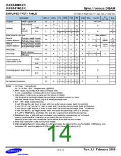
K4S640832K
K4S641632K
Synchronous DRAM
AC CHARACTERISTICS (AC operating conditions unless otherwise noted)
50
60
75
Parameter
Symbol
Unit Note
Min
Max
Min
6
Max
Min
7.5
10
-
Max
CAS latency=3
5
-
CLK cycle time
tCC
1000
1000
1000
ns
ns
ns
1
1,2
2
CAS latency=2
CAS latency=3
CAS latency=2
CAS latency=3
CAS latency=2
10
-
-
4.5
5
6
-
5.4
CLK to valid
output delay
tSAC
-
-
-
-
6
2
-
-
2.5
3
3
-
-
Output data
hold time
tOH
-
-
3
CLK high pulse width
CLK low pulse width
Input setup time
tCH
tCL
2
2
1.5
1
1
-
-
2.5
2.5
1.5
1
-
2.5
2.5
1.5
0.8
1
-
ns
ns
ns
ns
ns
3
3
-
-
-
tSS
-
-
-
3, 4
3, 4
2
Input hold time
tSH
tSLZ
-
-
-
-
CLK to output in Low-Z
1
-
-
CAS latency=3
CAS latency=2
4.5
-
-
5
6
-
5.4
6
CLK to output
in Hi-Z
tSHZ
ns
-
-
-
Notes :
1. Parameters depend on programmed CAS latency.
2. If clock rising time is longer than 1ns, (tr/2-0.5)ns should be added to the parameter.
3. Assumed input rise and fall time (tr & tf) = 1ns.
If tr & tf is longer than 1ns, transient time compensation should be considered,
i.e., [(tr + tf)/2-1]ns should be added to the parameter.
4. tSS applies for address setup time, clock enable setup time, commend setup time and data setup time
tSH applies for address holde time, clock enable hold time, commend hold time and data hold time
DQ BUFFER OUTPUT DRIVE CHARACTERISTICS
Parameter
Symbol
Condition
Min
Typ
Max
Unit
Notes
Measure in linear
region : 1.2V ~ 1.8V
Output rise time
trh
1.37
4.37
Volts/ns
3
Measure in linear
Output fall time
Output rise time
Output fall time
tfh
trh
tfh
1.30
2.8
3.8
5.6
5.0
Volts/ns
Volts/ns
Volts/ns
3
region : 1.2V ~ 1.8V
Measure in linear
region : 1.2V ~ 1.8V
3.9
2.9
1,2
1,2
Measure in linear
region : 1.2V ~ 1.8V
2.0
Notes :
1. Rise time specification based on 0pF + 50 Ω to VSS, use these values to design to.
2. Fall time specification based on 0pF + 50 Ω to VDD, use these values to design to.
3. Measured into 50pF only, use these values to characterize to.
4. All measurements done with respect to VSS.
Rev. 1.1 February 2006
11 of 14

 SAMSUNG [ SAMSUNG ]