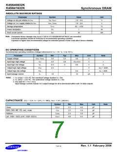
K4S640832K
K4S641632K
Synchronous DRAM
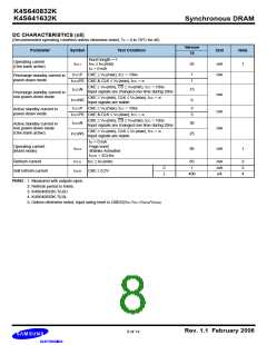
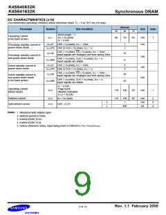
DC CHARACTERISTICS (x8)
(Recommended operating condition unless otherwise noted, TA = 0 to 70°C for x8)
Version
Parameter
Symbol
Test Condition
Unit
Note
75
Burst length = 1
tRC ≥ tRC(min)
IO = 0 mA
Operating current
ICC1
55
mA
mA
1
(One bank active)
ICC2P CKE ≤ VIL(max), tCC = 10ns
ICC2PS CKE & CLK ≤ VIL(max), tCC = ∞
1
1
Precharge standby current in
power-down mode
CKE ≥ VIH(min), CS ≥ VIH(min), tCC = 10ns
ICC2N
15
6
Input signals are changed one time during 20ns
Precharge standby current in
non power-down mode
mA
mA
mA
CKE ≥ VIH(min), CLK ≤ VIL(max), tCC = ∞
Input signals are stable
ICC2NS
ICC3P CKE ≤ VIL(max), tCC = 10ns
ICC3PS CKE & CLK ≤ VIL(max), tCC = ∞
3
3
Active standby current in
power-down mode
CKE ≥ VIH(min), CS ≥ VIH(min), tCC = 10ns
Input signals are changed one time during 20ns
ICC3N
30
25
Active standby current in
non power-down mode
(One bank active)
CKE ≥ VIH(min), CLK ≤ VIL(max), tCC = ∞
Input signals are stable
ICC3NS
IO = 0 mA
Operating current
(Burst mode)
Page burst
ICC4
80
mA
1
4Banks Activated
tCCD = 2CLKs
Refresh current
ICC5
ICC6
tRC ≥ tRC(min)
85
1
400
mA
mA
uA
2
3
4
C
L
Self refresh current
CKE ≤ 0.2V
Notes :
1. Measured with outputs open.
2. Refresh period is 64ms.
3. K4S640832K-T(U)C
4. K4S640832K-T(U)L
5. Unless otherwise noted, input swing IeveI is CMOS(VIH /VIL=VDDQ/VSSQ)
Rev. 1.1 February 2006
8 of 14

 SAMSUNG [ SAMSUNG ]