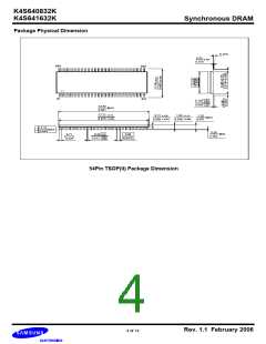
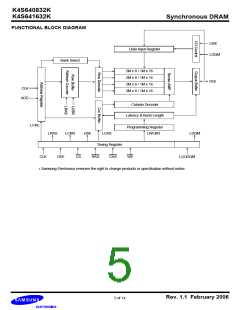
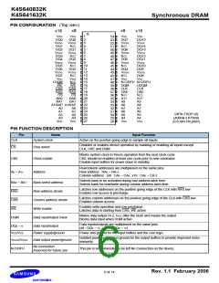
K4S640832K
K4S641632K
Synchronous DRAM
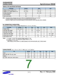
ABSOLUTE MAXIMUM RATINGS
Parameter
Voltage on any pin relative to VSS
Voltage on VDD supply relative to VSS
Storage temperature
Symbol
VIN, VOUT
VDD, VDDQ
TSTG
Value
Unit
-1.0 ~ 4.6
-1.0 ~ 4.6
-55 ~ +150
1
V
V
°C
W
Power dissipation
PD
Short circuit current
IOS
50
mA
Note :
Permanent device damage may occur if "ASOLUTE MAXIMUM RATINGS" are exceeded.
Functional operation should be restricted to recommended operating condition.
Exposure to higher than recommended voltage for extended periods of time could affect device reliability.
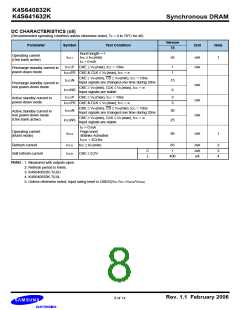
DC OPERATING CONDITIONS
Recommended operating conditions (Voltage referenced to VSS = 0V, TA = 0 to 70°C)
Parameter
Supply voltage
Symbol
VDD, VDDQ
VIH
Min
3.0
2.0
-0.3
2.4
-
Typ
3.3
3.0
0
Max
3.6
Unit
V
Note
Input logic high voltage
Input logic low voltage
Output logic high voltage
Output logic low voltage
Input leakage current
VDD+0.3
0.8
V
1
VIL
V
2
VOH
-
-
V
IOH = -2mA
IOL = 2mA
3
VOL
-
0.4
V
ILI
-10
-
10
uA
Notes :
1. VIH (max) = 5.6V AC.The overshoot voltage duration is ≤ 3ns.
2. VIL (min) = -2.0V AC. The undershoot voltage duration is ≤ 3ns.
3. Any input 0V ≤ VIN ≤ VDDQ.
Input leakage currents include Hi-Z output leakage for all bi-directional buffers with Tri-State outputs.
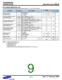
CAPACITANCE (VDD = 3.3V, TA = 23°C, f = 1MHz, VREF =1.4V ± 200 mV)
Pin
Symbol
CCLK
CIN
Min
2.5
2.5
2.5
4.0
Max
4.0
5.0
5.0
6.5
Unit
pF
Note
Clock
RAS, CAS, WE, CS, CKE, DQM
Address
pF
CADD
COUT
pF
(x8 : DQ0 ~ DQ7), (x16 : DQ0 ~DQ15)
pF
Rev. 1.1 February 2006
7 of 14

 SAMSUNG [ SAMSUNG ]