K4S640832K
K4S641632K
Synchronous DRAM
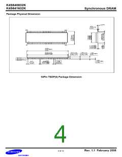
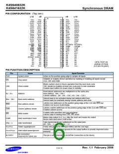
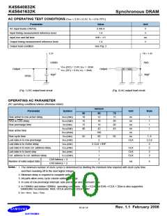
PIN CONFIGURATION (Top view)
x8
x8
x16
x16
VDD
DQ0
VDDQ
DQ1
DQ2
VSSQ
DQ3
DQ4
VDDQ
DQ5
DQ6
VSSQ
DQ7
VDD
VDD
DQ0
VDDQ
N.C
1
VSS
VSS
54
53
52
51
50
49
48
47
46
45
44
43
42
41
40
39
38
37
36
35
34
33
32
31
30
29
28
2
DQ7
VSSQ
N.C
DQ15
VSSQ
DQ14
DQ13
VDDQ
DQ12
DQ11
VSSQ
DQ10
DQ9
3
4
DQ1
VSSQ
N.C
5
DQ6
VDDQ
N.C
6
7
DQ2
VDDQ
N.C
8
DQ5
VSSQ
N.C
9
10
11
12
13
14
15
16
17
18
19
20
21
22
23
24
25
26
27
DQ3
VSSQ
N.C
DQ4
VDDQ
N.C
VDDQ
DQ8
VDD
VSS
VSS
LDQM
WE
N.C
N.C/RFU N.C/RFU
WE
DQM
CLK
CKE
N.C
A11
A9
UDQM
CLK
CKE
N.C
A11
A9
CAS
RAS
CS
CAS
RAS
CS
BA0
BA0
BA1
BA1
A10/AP A10/AP
A8
A8
A0
A1
A0
A1
A7
A7
A6
A6
54Pin TSOP (II)
(400mil x 875mil)
(0.8 mm Pin pitch)
A2
A2
A5
A5
A3
A3
A4
A4
VDD
VDD
VSS
VSS
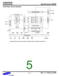
PIN FUNCTION DESCRIPTION
Pin
Name
Input Function
CLK
CS
System clock
Active on the positive going edge to sample all inputs.
Disables or enables device operation by masking or enabling all inputs except
CLK, CKE and DQM
Chip select
Masks system clock to freeze operation from the next clock cycle.
CKE should be enabled at least one cycle prior to new command.
Disable input buffers for power down in standby.
CKE
Clock enable
Row/column addresses are multiplexed on the same pins.
Row address : RA0 ~ RA11,
Column address : (x8 : CA0 ~ CA8 , x16 : CA0 ~ CA7)
A0 ~ A11
Address
Selects bank to be activated during row address latch time.
Selects bank for read/write during column address latch time.
Latches row addresses on the positive going edge of the CLK with RAS low.
Enables row access & precharge.
Latches column addresses on the positive going edge of the CLK with CAS low.
Enables column access.
Enables write operation and row precharge.
Latches data in starting from CAS, WE active.
BA0 ~ BA1
RAS
Bank select address
Row address strobe
Column address strobe
Write enable
CAS
WE
Makes data output Hi-Z, tSHZ after the clock and masks the output.
Blocks data input when DQM active.
DQM
Data input/output mask
Data inputs/outputs are multiplexed on the same pins.
(x8 : DQ0 ~ 7), (x16 : DQ0 ~ 15)
DQ0 ~ N
Data input/output
VDD/VSS
VDDQ/VSSQ
Power supply/ground
Data output power/ground
Power and ground for the input buffers and the core logic.
Isolated power supply and ground for the output buffers to provide improved noise
immunity.
No connection
/reserved for future use
N.C/RFU
This pin is recommended to be left No Connection on the device.
Rev. 1.1 February 2006
6 of 14

 SAMSUNG [ SAMSUNG ]