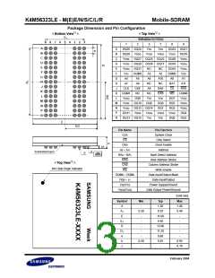
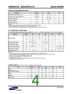
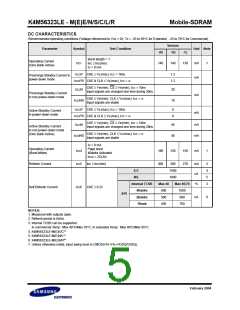
K4M56323LE - M(E)E/N/S/C/L/R
Mobile-SDRAM
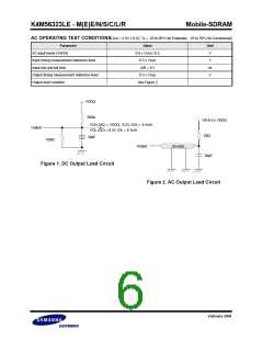
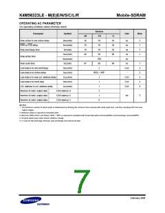
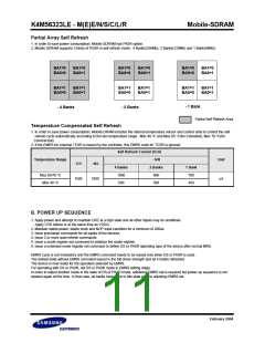
OPERATING AC PARAMETER
(AC operating conditions unless otherwise noted)
Version
Parameter
Symbol
Unit
Note
-80
16
19
19
48
-1H
-1L
19
24
24
60
Row active to row active delay
RAS to CAS delay
tRRD(min)
tRCD(min)
19
ns
ns
1
1
1
1
19
Row precharge time
tRP(min)
19
ns
tRAS(min)
50
ns
Row active time
tRAS(max)
100
us
Row cycle time
tRC(min)
67
69
84
ns
1
2
3
2
2
4
Last data in to row precharge
Last data in to Active delay
Last data in to new col. address delay
Last data in to burst stop
tRDL(min)
2
CLK
-
tDAL(min)
tRDL + tRP
tCDL(min)
1
1
1
2
1
0
CLK
CLK
CLK
tBDL(min)
Col. address to col. address delay
Number of valid output data
Number of valid output data
Number of valid output data
tCCD(min)
CAS latency=3
CAS latency=2
CAS latency=1
ea
5
NOTES:
1. The minimum number of clock cycles is determined by dividing the minimum time required with clock cycle time and then rounding off to the next
higher integer.
2. Minimum delay is required to complete write.
3. Minimum tRDL=2CLK and tDAL(= tRDL + tRP) is required to complete both of last data write command(tRDL) and precharge command(tRP).
4. All parts allow every cycle column address change.
5. In case of row precharge interrupt, auto precharge and read burst stop.
February 2004

 SAMSUNG [ SAMSUNG ]