K4M56323LE - M(E)E/N/S/C/L/R
Mobile-SDRAM
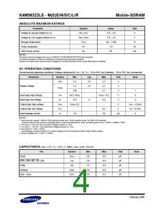
ABSOLUTE MAXIMUM RATINGS
Parameter
Symbol
VIN, VOUT
VDD, VDDQ
TSTG
Value
-1.0 ~ 3.6
-1.0 ~ 3.6
-55 ~ +150
1.0
Unit
V
Voltage on any pin relative to Vss
Voltage on VDD supply relative to Vss
Storage temperature
V
°C
W
Power dissipation
PD
Short circuit current
IOS
50
mA
NOTES:
Permanent device damage may occur if ABSOLUTE MAXIMUM RATINGS are exceeded.
Functional operation should be restricted to recommended operating condition.
Exposure to higher than recommended voltage for extended periods of time could affect device reliability.
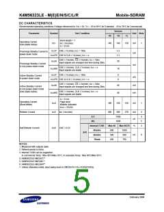
DC OPERATING CONDITIONS
Recommended operating conditions (Voltage referenced to VSS = 0V, TA = -25 to 85°C for Extended, -25 to 70°C for Commercial)
Parameter
Symbol
Min
2.3
Typ
Max
Unit
V
Note
VDD
2.5
2.7
Supply voltage
2.3
2.5
2.7
V
VDDQ
1.65
-
-
2.7
V
1
Input logic high voltage
Input logic low voltage
Output logic high voltage
Output logic low voltage
Input leakage current
NOTES :
VIH
VIL
0.8 x VDDQ
-0.3
VDDQ + 0.3
V
2
0
-
0.3
-
V
3
VOH
VOL
ILI
VDDQ -0.2
-
V
IOH = -0.1mA
IOL = 0.1mA
4
-
0.2
10
V
-10
-
uA
1. Samsung can support VDDQ 2.5V(in general case) and 1.8V(in specific case) for VDD 2.5V products.
Please contact to the memory marketing team in Samsung Electronics when considering the use of VDDQ 1.8V(Min 1.65V).
2. VIH (max) = 3.0V AC.The overshoot voltage duration is ≤ 3ns.
3. VIL (min) = -1.0V AC. The undershoot voltage duration is ≤ 3ns.
4. Any input 0V ≤ VIN ≤ VDDQ.
Input leakage currents include Hi-Z output leakage for all bi-directional buffers with tri-state outputs.
5. Dout is disabled, 0V ≤ VOUT ≤ VDDQ.
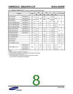
CAPACITANCE (VDD = 2.5V, TA = 23°C, f = 1MHz, VREF =0.9V ± 50 mV)
Pin
Symbol
CCLK
CIN
Min
3.0
3.0
1.5
3.0
3.0
Max
8.0
8.0
4.0
8.0
6.5
Unit
pF
Note
Clock
RAS, CAS, WE, CS, CKE
DQM
pF
CIN
pF
Address
CADD
COUT
pF
DQ0 ~ DQ31
pF
February 2004

 SAMSUNG [ SAMSUNG ]