256M GDDR3 SDRAM
K4J55323QG
10.0 AC & DC OPERATING CONDITIONS
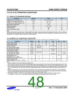
10.1 ABSOLUTE MAXIMUM RATINGS
Parameter
Voltage on any pin relative to Vss
Voltage on VDD supply relative to Vss
Voltage on VDDQ supply relative to Vss
MAX Junction Temperature
Storage temperature
Symbol
VIN, VOUT
VDD
VDDQ
TJ
Value
Unit
V
V
-0.5 ~ VDDQ + 0.5V
-0.5 ~ 2.5
-0.5 ~ 2.5
+125
V
°C
°C
W
TSTG
PD
-55 ~ +150
TBD
Power dissipation
Short Circuit Output Current
Note :
IOS
50
mA
Stresses greater than those listed under "Absolute Maximum Ratings" may cause permanent damage to the device. This is a stress rat-
ing only, and functional operation of the device at these or any other conditions above those indicated in the operational sections of this
specification is not implied. Exposure periods may affect reliability.
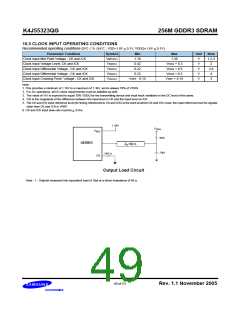
10.2 POWER & DC OPERATING CONDITIONS
Recommended operating conditions (Voltage referenced to 0°C ≤ Tc ≤ 85°C ; VDD=1.8V + 0.1V, VDDQ=1.8V + 0.1V)
Parameter
Device Supply voltage
Output Supply voltage
Symbol
VDD
VDDQ
Min
1.7
1.7
0.69*VDDQ
Typ
1.8
1.8
-
-
-
-
-
-
-
Max
1.9
Unit
V
V
V
V
V
V
V
V
Note
1
1
2
3
3
1.9
0.71*VDDQ
-
VREF-0.15
0.76
Reference voltage
VREF
DC Input logic high voltage
DC Input logic low voltage
Output logic low voltage
AC Input logic high voltage
AC Input logic low voltage
Input leakage current
Any input 0V-<VIN -< VDDQ
(All other pins not under test = 0V)
VIH (DC)
VIL (DC)
VOL(DC)
VIH(AC)
VIL(AC)
VREF+0.15
-
-
VREF+0.25
-
-
3,4,5
3,4,5
VREF-0.25
uA
II
-5
-5
5
5
Output leakage current
(DQs are disabled ; 0V-<VOUT -< VDDQ)
IIOZ
-
uA
Note :
1. Under all conditions, VDDQ must be less than or equal to VDD.
2. VREF is expected to equal 70% of VDDQ for the transmitting device and to track variations in the DC level of the same. Peak-to-peak noise on VREF
may not exceed + 2 percent of the DC value. Thus, from 70% of VDDQ, VREF is allowed + 25mV for DC error and an additional +25mV for AC noise.
3. The DC values define where the input slew rate requirements are imposed, and the input signal must not violate these levels in order to maintain a valid
level. The inputs require the AC value to be achieved during signal transition edge and the driver should achieve the same slew rate through the AC
values.
4. Input and output slew rate =3V/ns. If the input slew rate is less than 3V/ns, input timing may be compromised. All slew rate are measured between
Vih and Vil. DQ and DM input slew rate must not deviate from DQS by more than 10%. If the DQ,DM and DQS slew rate is less than 3V/ns, timing is
longer than referenced to the mid-point but to the VIL(AC) maximum and VIH(AC) minimum points.
5. VIH overshoot : VIH(max) = VDDQ + 0.5V for a pulse width ≤ 500ps and the pulse width can not be greater than 1/3 of the cycle rate.
VIL undershoot : VIL(min)=0.0V for a pulse width ≤ 500ps and the pulse width can not be greater than 1/3 of the cycle rate.
48 of 53
Rev. 1.1 November 2005

 SAMSUNG [ SAMSUNG ]