256M GDDR3 SDRAM
K4J55323QG
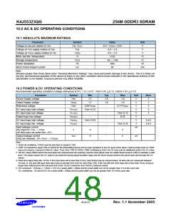
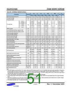
10.6 AC CHARACTERISTICS(I-I)
-12
-14
-16
-20
Parameter
Symbol
Unit Note
Min
-0.23
0.45
0.45
1.25
1.4
Max
+0.23
0.55
Min
-0.26
0.45
0.45
Max
Min
Max
Min
Max
t
DQS out access time from CK
CK high-level width
CK low-level width
CL=11
+0.26 -0.29 +0.29 -0.35 +0.35
ns
tCK
tCK
ns
DQSCK
t
0.55
0.55
0.45
0.45
-
0.55
0.55
0.45
0.45
-
-
-
0.55
0.55
CH
t
0.55
CL
CL=10
1.4
1.6
2.0
2.0
5
ns
-
CK cycle time
CL=9
CL=8
CL=7
1.6
3.3
3.3
ns
1.6
2.0
2.0
5
3.3
3.3
t
t
CK
2.0
ns
-
2.0
ns
2.0
4
WRITE Latency
6
-
-
-
-
tCK
ns
1
WL
t
DQ and DM input hold time relative to DQS
DQ and DM input setup time relative to DQS
Active termination setup time
Active termination hold time
DQS input high pulse width
0.16
0.16
10
-
0.18
0.18
10
-
0.20
0.20
10
-
0.25
0.25
10
-
DH
t
-
-
-
-
-
-
-
-
ns
DS
t
t
ns
ATS
10
-
10
-
10
0.48
0.48
-
10
0.48
0.48
-
ns
ATH
tDQSH
tDQSL
0.48
0.48
0.52
0.52
0.48
0.48
0.52
0.52
tCK
tCK
ns
0.52
0.52
0.52
0.52
DQS input low pulse widthl
Data strobe edge to Dout edge
DQS read preamble
tDQSQ -0.140 0.140 -0.160 0.160
0.180 0.180 0.225 0.225
0.4
0.4
tRPRE
tRPST
0.4
0.4
0.6
0.6
0.4
0.4
0.6
0.6
tCK
tCK
tCK
tCK
ns
0.6
0.6
0.4
0.4
0.6
0.6
DQS read postamble
WL-0.2 WL+0.2 WL-0.2 WL+0.2
tDQSS WL-0.2 WL+0.2 WL-0.2 WL+0.2
Write command to first DQS latching transition
DQS write preamble
tWPRE
tWPRES
tWPST
0.35
0
-
-
0.4
0
0.6
-
2
3
0.4
0
0.4
0.6
-
0.6
0.4
0
0.4
0.6
-
0.6
DQS write preamble setup time
DQS write postamble
0.4
0.6
0.4
0.6
tCK
tCLmin
or
tCLmin
or
tCLmin
or
tCLmin
or
Half strobe period
tHP
tQH
-
-
-
-
-
-
-
tCK
ns
tCHmin
tCHmin
tCHmin
tCHmin
tHP
-
tHP-
0.225
t
-
t
-
HP
HP
Data output hold time from DQS
-
0.14
0.16
0.18
Data-out high-impedance window
from CK and /CK
tHZ
tLZ
-0.3
-
-
-0.3
-
-
-0.3
-
-
-0.3
-
-
ns
ns
4
4
Data-out low-impedance window from
CK and /CK
-0.3
-0.3
-0.3
-0.3
Address and control input hold time
Address and control input setup time
Address and control input pulse width
Jitter over 1~6 clock cycle error
Cycle to cyde duty cycle error
Rise and fall times of CK
tIH
tIS
0.3
0.3
0.9
-
-
-
0.35
-
-
ns
ns
0.4
0.4
1.1
-
-
-
-
-
-
0.5
0.5
1.3
-
-
-
-
-
-
0.35
tIPW
tJ
-
1.0
-
ns
0.03
0.03
0.2
-
-
-
0.03
0.03
0.2
0.03
0.03
0.2
0.03
0.03
0.2
tCK
tCK
tCK
5
tDCERR
tR, tF
-
-
Note :
1. The WRITE latency can be set from 1 to 7 clocks. When the WRITE latency is set to 1 or 2 or 3 clocks(this case can be used regardless of frequency),
the input buffers are turned on during the ACTIVE commands reducing the latency but added power. When the WRITE latency is set to 4 ~7 clocks ,
the input buffers are turned on during the WRITE commands for lower power operation. The WRITE latency which is over 4 clocks can be used only in
case that Write Latency*tCK is greater than 7ns.
2. A low to high transition on the WDQS line is not allowed in the half clock prior to the write preamble.
3. The last rising edge of WDQS after the write postamble must be riven high by the controller. WDQS can not be pulled high by the on-die termination
alone.
4. tHZ and tLZ transitions occur in the same access time windows as valid data transitions. These parameters are not referenced to a specific voltage
level, but specify when the device output is no longer driving (HZ) or begins driving (LZ).
5. The cycle to cycle jitter over 1~6 cycle short term jitter
51 of 53
Rev. 1.1 November 2005

 SAMSUNG [ SAMSUNG ]