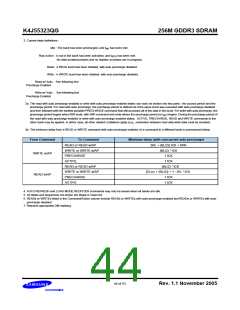
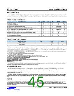
256M GDDR3 SDRAM
K4J55323QG
DATA TERMINATION DISABLE
(BUS SNOOPING FOR READ COMMAND)
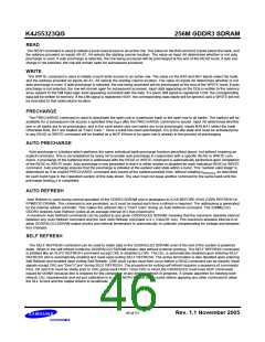
The DATA TERMINATOR DISABLE COMMAND is detected by the device by snooping the bus for READ commands excluding /CS.
The GDDR3 DRAM will disable its Data terminators when a READ command is detected. The terminators are disable CL-1 Clocks after
the READ command is detected. In a two rank system both dram devices will snoop the bus for READ commands to either device and
both will disable their terminators if a READ command is detected. The command and address terminators and always enabled.
ON-DIE TERMINATION
Bus snooping for READ commands other than /CS is used to control the on-die termination in the dual load configuration. The GDDR3
SDRAM will disable the on-die termination when a READ command is detected, regardless of the state of
/CS, when the ODT for the DQ pins are set for dual loads (120Ω). The on-die termination is disabled x clocks after the READ command
where x equals CL-1 and stay off for a duration of BL/2 + 2, as below figure, Data Termination Disable Timing. In a two-rank system, both
DRAM devices snoop the bus for READ commands to either device and both will disable the on-die termination if a READ command is
detected. The on-die termination for all other pins on the device are always on for both a single-rank system and a dual-rank system.
The on-die termination value on address and control pins is determined during power-up in relation to the state of CKE on the first tran-
sition of RESET. On the rising edge of RESET, if CKE is sampled LOW, then the configuration is determined to be a single-rank system.
The on-die termination is then set to one-half ZQ for the address pins. On the rising edge of RESET, if CKE is sampled HIGH, then the
configuration is determined to be a dual-rank system. The on-die termination for the DQs, WDQS, and DM pins is set in the EMRS.
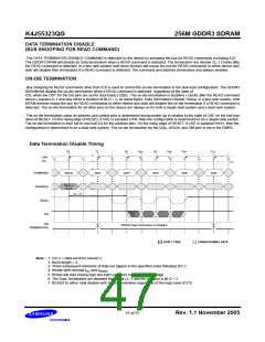
Data Termination Disable Timing
T0
T7
T8
T8n
T9
T9n
T10
T11
CK#
CK
COMMAND
ADDRESS
READ
NOP
NOP
NOP
NOP
NOP
Bank a,
Col n
CL = 8
RDQS
DQ
DO
n
DQ
GDDR3 Data Termination is Disabled
TERMINATION
DON’T CARE
TRANSITIONING DATA
Note : 1. DO n = data-out from column n.
2. Burst length = 4.
3. Three subsequent elements of data-out appear in the specified order following DO n.
4. Shown with nominal tAC and tDQSQ
.
5. RDQS will start driving high one-half cycle prior to the first falling edge.
6. The Data Terminators are disabled starting at CL-1 and the duration is BL/2 + 2
7. READS to either rank disable both ranks’ termination regardless of the logic level of /CS.
47 of 53
Rev. 1.1 November 2005

 SAMSUNG [ SAMSUNG ]