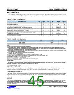
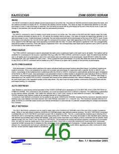
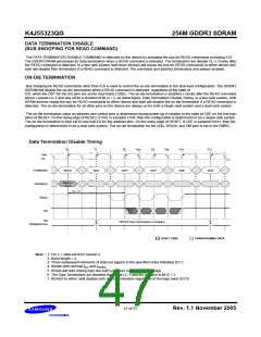
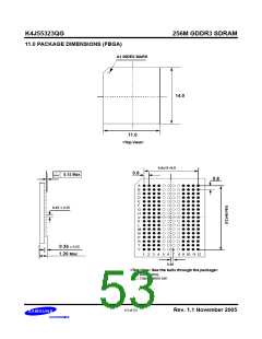
256M GDDR3 SDRAM
K4J55323QG
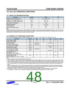
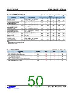
10.3 CLOCK INPUT OPERATING CONDITIONS
Recommended operating conditions (0°C ≤ Tc ≤85°C ; VDD=1.8V + 0.1V, VDDQ=1.8V + 0.1V)
Parameter/ Condition
Clock Input Mid-Point Voltage ; CK and /CK
Clock Input Voltage Level; CK and /CK
Clock Input Differential Voltage ; CK and /CK
Clock Input Differential Voltage ; CK and /CK
Clock Input Crossing Point Voltage ; CK and /CK
Symbol
VMP(DC)
VIN(DC)
VID(DC)
VID(AC)
VIX(AC)
Min
1.16
0.42
0.22
0.22
Max
1.36
VDDQ + 0.3
VDDQ + 0.5
VDDQ + 0.3
VREF + 0.15
Unit
V
V
V
V
Note
1,2,3
2
2,4
4
VREF - 0.15
V
3
Note :
1. This provides a minimum of 1.16V to a maximum of 1.36V, and is always 70% of VDDQ
2. For AC operations, all DC clock requirements must be satisfied as well.
3. The value of VIX is expected to equal 70% VDDQ for the transmitting device and must track variations in the DC level of the same.
4. VID is the magnitude of the difference between the input level in CK and the input level on /CK.
5. The CK and /CK input reference level (for timing referenced to CK and /CK) is the point at which CK and /CK cross; the input reference level for signals
other than CK and /CK is VREF.
6. CK and /CK input slew rate must be > 3V/ns
1.26V
VDDQ
VREF
60
Ω
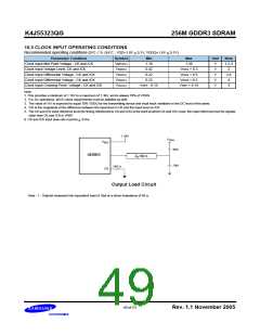
GDDR3
Z =60
Ω
0
10pf
240
Ω
ZQ
Output Load Circuit
Note : 1 . Outputs measured into equivalent load of 10pf at a driver impedance of 40 Ω.
49 of 53
Rev. 1.1 November 2005

 SAMSUNG [ SAMSUNG ]