256M GDDR3 SDRAM
K4J55323QG
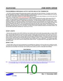
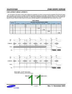
CAS LATENCY (READ LATENCY)
The CAS latency is the delay, in clock cycles, between the registration of a READ command and the availability of the first bit of output
data. The latency can be set to 4~15 clocks. If a READ command is registered at clock edge n, and the latency is m clocks, the data will
be available nominally coincident with clock edge n+m. Below table indicates the operating frequencies at which each CAS latency set-
ting can be used. Reserved states should not be used as unknown operation or incompatibility with future versions may result.
CAS Latency
Allowable operating frequency (MHz)
SPEED
CL=15
CL=14
CL=13
CL=12
CL=11
CL=10
CL=9
CL=8
CL=7
-10
-11
-12
-14
-16
-20
TBD
TBD
≤ 800
-
-
-
-
-
-
-
-
-
-
≤ 700
-
-
-
-
≤ 600
≤ 500
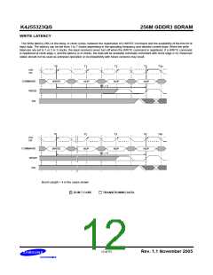
T0
T5
T6
T7
T7n
/CK
CK
COMMAND
RDQS
READ
NOP
NOP
NOP
CL = 7
DQ
T0
T6
T7
T8
T8n
/CK
CK
COMMAND
RDQS
READ
NOP
NOP
NOP
CL = 8
DQ
Burst Length = 4 in the cases shown
Shown with nominal tAC and nominal tDSDQ
DON’T CARE
TRANSITIONING DATA
11 of 53
Rev. 1.1 November 2005

 SAMSUNG [ SAMSUNG ]