64M DDR SDRAM
K4D64163HF
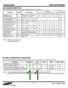
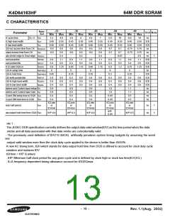
DC CHARACTERISTICS
Recommended operating conditions Unless Otherwise Noted, TA=0 to 65°C)
Version
Parameter
Symbol
Test Condition
Unit Note
-33
-36
-40
-50
-60
Burst Lenth=2 tRC ≥ tRC(min)
IOL=0mA, tCC= tCC(min)
Operating Current
(One Bank Active)
ICC1
210
200
190
170
160
mA
mA
mA
mA
mA
mA
1
Precharge Standby Current
in Power-down mode
ICC2P
ICC2N
ICC3P
ICC3N
ICC4
5
CKE ≤ VIL(max), tCC= tCC(min)
CKE ≥ VIH(min), CS ≥ VIH(min),
tCC= tCC(min)
Precharge Standby Current
in Non Power-down mode
110
110
160
105
105
150
95
80
80
70
70
Active Standby Current
power-down mode
95
CKE ≤ VIL(max), tCC= tCC(min)
CKE ≥ VIH(min), CS ≥ VIH(min),
tCC= tCC(min)
Active Standby Current in
in Non Power-down mode
140
350
120
100
Operating Current
( Burst Mode)
tRC ≥ tRFC(min)tRC ≥ tRFC(min)
Page Burst, All Banks activated.
390
210
370
200
320
180
300
170
Refresh Current
ICC5
ICC6
190
2
mA
mA
2
tRC ≥ tRFC(min)
CKE ≤ 0.2V
Self Refresh Current
Note : 1. Measured with outputs open.
2. Refresh period is 64ms.
AC INPUT OPERATING CONDITIONS
Recommended operating conditions(Voltage referenced to VSS=0V, VDD=3.3V+ 5%, VDDQ=2.5V+ 5%,TA=0 to 65°C)
Parameter
Symbol
VIH
Min
VREF+0.35
-
Typ
Max
-
Unit
Note
Input High (Logic 1) Voltage; DQ
-
-
-
-
V
V
V
V
Input Low (Logic 0) Voltage; DQ
VIL
VREF-0.35
VDDQ+0.6
0.5*VDDQ+0.2
Clock Input Differential Voltage; CK and CK
Clock Input Crossing Point Voltage; CK and CK
VID
0.7
1
2
VIX
0.5*VDDQ-0.2
Note : 1. VID is the magnitude of the difference between the input level on CK and the input level on CK
2. The value of VIX is expected to equal 0.5*VDDQ of the transmitting device and must track variations in the DC level of the same
- 11 -
Rev. 1.1(Aug. 2002)

 SAMSUNG [ SAMSUNG ]