64M DDR SDRAM
K4D64163HF
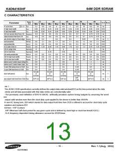
C CHARACTERISTICS
-33
-36
-40
-50
-60
Sym-
Unit Note
Parameter
bol
Min
3.3
0.45
0.45
-0.6
-0.6
-
Max
4.0
0.55
0.55
0.6
0.6
0.4
1.1
0.6
1.25
-
Min
3.6
0.45
0.45
-0.6
-0.6
-
Max
6
Min
4.0
0.45
0.45
-0.6
-0.6
-
Max
7
Min
5.0
0.45
0.45
-0.7
-0.7
-
Max
10
0.55
0.55
0.7
0.7
0.45
1.1
0.6
1.2
-
Min
6.0
Max
10
0.55
0.55
0.75
0.75
0.5
1.1
0.6
1.25
-
K cycle time
CL=3
ns
tCK
tCK
ns
tCK
tCH
tCL
K high level width
K low level width
0.55
0.55
0.6
0.6
0.4
1.1
0.6
1.15
-
0.55
0.55
0.6
0.6
0.4
1.1
0.6
1.15
-
0.45
0.45
-0.75
-0.75
-
QS out access time from CK
utput access time from CK
ata strobe edge to Dout edge
ead preamble
tDQSCK
tAC
ns
ns
1
tDQSQ
tRPRE
tRPST
tDQSS
tWPRES
tWPREH
tWPST
tDQSH
tDQSL
tIS
0.9
0.4
0.8
0
0.9
0.4
0.85
0
0.9
0.4
0.85
0
0.9
0.4
0.8
0
0.9
tCK
tCK
tCK
ns
ead postamble
0.4
K to valid DQS-in
0.75
0
QS-In setup time
QS-in hold time
0.45
0.4
0.4
0.4
0.9
0.9
0.4
0.4
-
0.35
0.4
0.4
0.4
0.9
0.9
0.4
0.4
-
0.35
0.4
0.4
0.4
0.9
0.9
0.4
0.4
-
0.3
0.4
0.4
0.4
1.0
1.0
0.45
0.45
-
0.25
0.4
-
tCK
tCK
tCK
tCK
ns
QS write postamble
0.6
0.6
0.6
-
0.6
0.6
0.6
-
0.6
0.6
0.6
-
0.6
0.6
0.6
-
0.6
0.6
0.6
-
QS-In high level width
QS-In low level width
ddress and Control input setup
ddress and Control input hold
Q and DM setup time to DQS
Q and DM hold time to DQS
0.4
0.4
1.1
-
-
-
-
1.1
-
ns
tIH
tDS
tDH
-
-
-
-
0.5
-
ns
-
-
-
-
0.5
-
ns
tCLmin
or
tCHmin
tCLmin
or
tCHmin
tCLmin
or
tCHmin
tCLmin
or
tCHmin
tCLmin
or
tCHmin
lock half period
-
-
-
-
-
-
-
-
-
ns
ns
1
1
tHP
tQH
tHP-
0.45
ata output hold time from DQS
tHP-0.4
tHP-0.4
tHP-0.4
tHP-0.5
ote 1 :
The JEDEC DDR specification currently defines the output data valid window(tDV) as the time period when the data
strobe and all data associated with that data strobe are coincidentally valid.
- The previously used definition of tDV(=0.35tCK) artificially penalizes system timing budgets by assuming the worst
ase
output vaild window even then the clock duty cycle applied to the device is better than 45/55%
A new AC timing term, tQH which stands for data output hold time from DQS is difined to account for clock duty cycle
variation and replaces tDV
tQHmin = tHP-X where
. tHP=Minimum half clock period for any given cycle and is defined by clock high or clock low time(tCH,tCL)
. X=A frequency dependent timing allowance account for tDQSQmax
- 13 -
Rev. 1.1(Aug. 2002)

 SAMSUNG [ SAMSUNG ]