2X20 LCD Compatible VFD Module
20T202DA1E (Rev. 3.0)
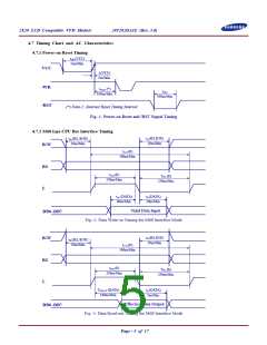
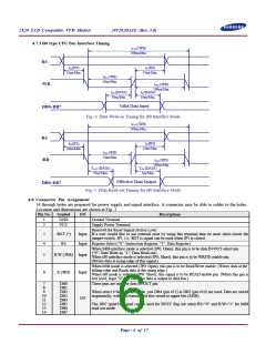
4.7.3 i80 type CPU Bus Interface Timing
tCYC(/WR)
200ns/Min.
RS
tH (RS)
tSU(RS)
10ns/Min.
10ns/Min.
tWL (/WR)
30ns/Min.
/WR
tWH (/WR)
100ns/Min.
tSU (DATA)
30ns/Min.
tH (DATA)
10ns/Min.
Valid Data Input
DB0~DB7
Fig.-4. Data Write-in Timing for i80 Interface Mode
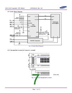
tCYC(/WR)
200ns/Min.
RS
tH (RS)
tSU(RS)
10ns/Min.
tWL (/RD)
10ns/Min.
70ns/Min.
tWH (/RD)
/RD
100ns/Min.
TACC (DATA)
70ns/Max.
T
OH (DATA)
5ns/Min.
Effective Data Output
Fig.-5. Data Read-out Timing for i80 Interface Mode
DB0~DB7
4.8 Connector Pin Assignment
14 through holes are prepared for power supply and signal interface. A connector may be able to solder to the holes.
Location and dimensions are shown at Fig.-7.
Pin No.
Symbol
I/O
Descriptions
1
2
GND
-
-
Ground Terminal
VCC
Supply Power Terminal
Reserved for Reset Signal (Active Low)
Input If a user would like to use external reset by using this terminal then he must short-circuit the
3
4
/RST (*)
RS
jumper switch, JP1. i.e. /RST is signal can be used when JP1 is closed.
Input Register Select ("0"; Instruction Register, "1"; Data Register)
When M68 interface mode is selected (JP0; Open), this pin is to be data IN/OUT select pin.
("0"; Data Write-in, "1"; Data Read-out)
When i80 interface mode is selected (JP0; Short), this pin is to be WRITE enable pin.
(Writes data at rising edge of this signal.)
5
6
R/W (/WR) Input
When M68 mode is selected (JP0; Open), this pin is to be Read/Write enable. (Writes data at the
falling edge and Reads data at the rising edge.)
When i80 mode is selected (JP0: Short), this signal is to be READ enable pin. (When this pin is
low level, logic "0", the effective data is output to data bus.)
E (/RD)
Input
I/O
7
8
9
10
11
12
13
14
DB0
DB1
DB2
DB3
DB4
DB5
DB6
DB7
These pins are used for data IN/OUT pin.
When select 4 bits transfer mode, just DB4 (pin #11) to DB7 (pin #14) are used. Data are stored
sequentially, with data transmitted first stored in upper bits (MSB).
The DB7 (pin#14) signal can be used for BUSY flag out when RS="0" and R/W="1" for M68
read-out mode.
Page - 6 of 17

 SAMSUNG [ SAMSUNG ]