Data Sheet
AD7656-1/AD7657-1/AD7658-1
If it is required to clock conversion data out on two data output
lines, use DOUT A and DOUT B. To enable DOUT A and
DOUT B, tie DB0/SEL A and DB1/SEL B to VDRIVE, and
DB2/SEL C should be tied low. When six simultaneous conversions
are performed and only two DOUT lines are used, a 48-SCLK
transfer can be used to access the data from the AD7656-1/
AD7657-1/AD7658-1. Any additional SCLKs applied after this
result in an output of all zeros. The read sequence is shown in
Figure 33 for a simultaneous conversion on all six ADCs using
two DOUT lines. If a simultaneous conversion occurred on all
six ADCs, and only two DOUT lines are used to read the results
from the AD7656-1/AD7657-1/AD7658-1, DOUT A clocks out
the result from V1, V2, and V5, whereas DOUT B clocks out
the results from V3, V4, and V6.
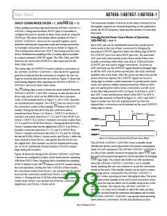
CHANGING THE ANALOG INPUT RANGE
(H/S SEL = 0)
The AD7656-1/AD7657-1/AD7658-1 RANGE pin allows the
user to select either 2 × VREF or 4 × VREF as the analog input
H
range for the six analog inputs. When the /S SEL pin is low,
the logic state of the RANGE pin is sampled on the falling edge of
the BUSY signal to determine the range for the next simultaneous
conversion. When the RANGE pin is logic high at the falling
edge of the BUSY signal, the range for the next conversion is
2 × VREF. When the RANGE pin is logic low at the falling
edge of the BUSY signal, the range for the next conversion is
4 × VREF. After a RESET pulse, the range is updated on the first
falling BUSY edge.
CHANGING THE ANALOG INPUT RANGE
(H/S SEL = 1)
Data can also be clocked out using just one DOUT line, in which
case useDOUT A to access the conversion data. To configure
the AD7656-1/AD7657-1/AD7658-1 to operate in this mode,
tie DB0/SEL A to VDRIVE, and tie DB1/SEL B and DB2/SEL C
low. The disadvantage of using only one DOUT line is that the
throughput rate is reduced. Data can be accessed from the
AD7656-1/AD7657-1/AD7658-1 using one 96-SCLK transfer,
three 32-SCLK individually framed transfers, or six 16-SCLK
individually framed transfers. Any additional SCLKs applied
after this result in an output of all zeros. When using the serial
H
When the /S SEL pin is high, the range can be changed by
writing to the control register. DB[12:10] in the control register
are used to select the analog input ranges for the next conversion.
Each analog input pair has an associated range bit, allowing
independent ranges to be programmed on each ADC pair. When
the RNGx bit is set to 1, the range for the next conversion is
× VREF. When the RNGx bit is set to 0, the range for the next
conversion is 4 × VREF.
2
RD
interface, tie the
unconnected.
signal low and leave the unused DOUT line(s)
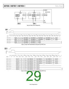
Serial Interface (SER/
SEL = 1)
PAR
By pulsing one, two, or all three CONVST signals, the AD7656-1/
AD7657-1/AD7658-1 use their on-chip trimmed oscillator to
simultaneously convert the selected channel pairs on the rising
edge of CONVST. After the rising edge of CONVST, the BUSY
signal goes high to indicate that the conversion has started. It
returns low when the conversion is complete, 3 µs later. Any
further CONVST rising edges on either CONVST A, CONVST B,
or CONVST C are ignored as long as BUSY is high. The output
register is loaded with the new conversion results, and data can
be read from the AD7656-1/AD7657-1/AD7658-1. To read the
Whether one, two, or three data output lines are used, if a
particular CONVST pin is not used in the conversion cycle then
all zeros are output in place of the ADC result for the associated
ADCs even though they were not used in the conversion cycle.
This means that if, for example, only CONVST B is pulsed and
one data output pin is in use, then 64 SCLKs are required to
access the results from V3 and V4, but only 32 SCLKs are
required if two or three data output lines are in use.
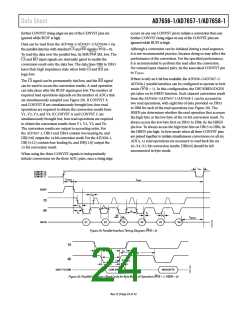
SERIAL READ OPERATION
PAR
data back from the parts over the serial interface, SER/
SEL
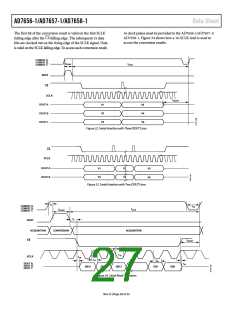
Figure 34 shows the timing diagram for reading data from the
AD7656-1/AD7657-1/AD7658-1 when the serial interface is
selected. The SCLK input signal provides the clock source for
should be tied high. The and SCLK signals are used to transfer
CS
data from the AD7656-1/AD7657-1/AD7658-1. The parts have
three DOUT pins: DOUT A, DOUT B, and DOUT C. Data
can be read back from each part using one, two, or all three
DOUT lines.
CS
the serial interface. The
signal goes low to access data from
CS
the AD7656-1/AD7657-1/AD7658-1. The falling edge of
takes the bus out of three-state and clocks out the MSB of the
16-bit conversion result. The ADCs output 16 bits for each
conversion result; the data stream of the AD7656-1 consists of
16 bits of conversion data, provided MSB first. The data stream
for the AD7657-1 consists of two leading 0s followed by 14 bits
of conversion data, provided MSB first. The data stream for the
AD7658-1 consists of four leading 0s and 12 bits of conversion
data, provided MSB first.
Figure 32 shows six simultaneous conversions and the read
sequence using three DOUT lines. Also in Figure 32, 32 SCLK
transfers are used to access data from the AD7656-1/AD7657-1/
AD7658-1; however, two 16-SCLK individually framed transfers
CS
with the
signal can also be used to access the data on the
three DOUT lines. Any additional SCLKs applied after this
result in an output of all zeros. When the serial interface is
selected and conversion data is clocking out on all three DOUT
lines, tie DB0/SEL A, DB1/SEL B, and DB2/SEL C to VDRIVE
.
These pins are used to enable the DOUT A to DOUT C lines,
respectively.
Rev. D | Page 25 of 32

 ROCHESTER [ Rochester Electronics ]