Data Sheet
AD7656-1/AD7657-1/AD7658-1
The maximum number of devices in the chain is limited by the
throughput required per channel depending on the application
needs, the SCLK frequency used, and the number of serial data
lines used.
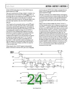
DAISY-CHAIN MODE (DCEN = 1, SER/PAR SEL = 1)
When reading conversion data back from the AD7656-1/AD7657-1/
AD7658-1 using one/two/three DOUT pins, it is possible to
configure the parts to operate in daisy-chain mode by using the
DCEN pin. This daisy-chain feature allows multiple AD7656-1/
AD7657-1/AD7658-1 devices to be cascaded together and is
useful for reducing the component count and wiring connections.
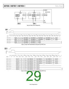
An example connection of two devices is shown in Figure 36.
This configuration shows two DOUT lines being used for each
device. Simultaneous sampling of the 12 analog inputs is possible
by using a common CONVST signal. The DB5, DB4, and DB3
data pins are used as the DCIN[A:C] data input pins for the
daisy-chain mode.
Standby/Partial Power-Down Modes of Operation
PAR
(SER/
SEL = 0 or 1)
Each ADC pair can be individually placed into partial power-
down mode at the end of their conversion by bringing the
associated CONVST signal low before the falling edge of BUSY.
If a CONVST pin is low when BUSY goes low, the associated
ADC pair only enters partial power-down mode if they were
actually converting within that cycle, that is, if that particular
CONVST pin was used to trigger conversions. To power an
ADC pair back up, the CONVST signal should be brought high
to tell the ADC pair to power up and place the track-and-hold
amplifier into track mode. After the power-up time from partial
power-down has elapsed, the CONVST signal can receive a
rising edge to initiate a valid conversion. In partial power-down
mode, the reference buffers remain powered up. When an ADC
pair is in partial power-down mode, conversions can still occur
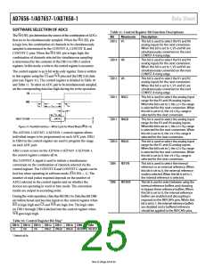
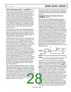
on the other fully powered ADCs. In Figure 35 at Point A, ADC 1
and ADC 2 enter partial power-down while ADC 3 to ADC 6
remain fully powered. At Point B in Figure 35, ADC1 and ADC 2
begin to power up. Once the required power up time has
elapsed then a conversion can be initiated on the next CONVST
rising edge as shown.
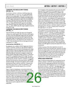
The rising edge of CONVST is used to initiate a conversion on
the AD7656-1/AD7657-1/AD7658-1. After the BUSY signal has
gone low to indicate that the conversion is complete, the user can
begin to read the data from the two devices. Figure 37 shows the
serial timing diagram when operating two AD7656-1/AD7657-1/
AD7658-1 devices in daisy-chain mode.
CS
The
falling edge is used to frame the serial transfer from the
AD7656-1/AD7657-1/AD7658-1 devices, to take the bus out of
three-state, and to clock out the MSB of the first conversion
result. In the example shown in Figure 37, all 12 ADC channels
are simultaneously sampled. Two DOUT lines are used to read
CS
the conversion results in this example. frames a 96-SCLK
transfer. During the first 48 SCLKs, the conversion data is
transferred from Device 2 to Device 1. DOUT A on Device 2
transfers conversion data from V1, V2, and V5 into DCIN A in
Device 1; DOUT B on Device 2 transfers conversion results from
V3, V4, and V6 to DCIN B in Device 1. During the first 48 SCLKs,
Device 1 transfers data into the digital host. DOUT A on Device 1
transfers conversion data from V1, V2, and V5; DOUT B on
Device 1 transfers conversion data from V3, V4, and V6. During
the last 48 SCLKs, Device 2 clocks out 0s, and Device 1 shifts the
data clocked in from Device 2 during the first 48 SCLKs into
the digital host. This example can also be implemented using
six 16-SCLK individually framed transfers if DCEN remains
high during the transfers.
A
B
tWAKE-UP
CONVST A
BUSY
CONVST B
CONVST C
Figure 35. Entering and Exiting Partial Power-Down Mode
The AD7656-1/AD7657-1/AD7658-1 have a standby mode
whereby the devices can be placed into a low power consumption
mode (315 μW maximum). The AD7656-1/AD7657-1/AD7658-1
STBY
are placed into standby mode by bringing the input
low and can be powered up again for normal operation by bringing
STBY
logic
Figure 38 shows the timing if two AD7656-1/AD7657-1/AD7658-
1 devices are configured in daisy-chain mode and are operating
with three DOUT lines. Assuming that a simultaneous sampling
logic high. The output data buffers are still operational
when the AD7656-1/AD7657-1/AD7658-1 are in standby
mode, meaning the user can continue to access the conversion
results of the parts. This standby feature can be used to reduce
the average power consumed by the AD7656-1/AD7657-1/
AD7658-1 when operating at lower throughput rates. The parts
can be placed into standby at the end of each conversion when
BUSY goes low and are taken out of standby mode prior to the
next conversion. The time for the AD7656-1/AD7657-1/
AD7658-1 to come out of standby is called the wake-up time.
The wake-up time limits the maximum throughput rate at which
the AD7656-1/AD7657-1/AD7658-1 can operate when powering
down between conversions. See the Specifications section.
CS
of all 12 inputs occurs, the
frames a 64 SCLK transfer during
the read operation. During the first 32 SCLKs of this transfer,
the conversion results from Device 1 are clocked into the digital
host and the conversion results from Device 2 are clocked into
Device 1. During the last 32 SCLKs of the transfer, the conversion
results from Device 2 are clocked out of Device 1 and into the
digital host, and Device 2 clocks out 0s.
Rev. D | Page 27 of 32

 ROCHESTER [ Rochester Electronics ]