AD7656-1/AD7657-1/AD7658-1
Data Sheet
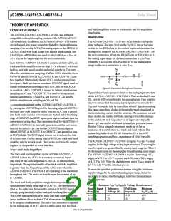
DV
CC
+
DIGITAL SUPPLY
VOLTAGE +3V OR +5V
ANALOG SUPPLY
VOLTAGE 5V
+
+
1µF
1µF
1µF
AGND AV
DV
DGND
V
DGND
DRIVE
CC
CC
1
+9.5V TO +16.5V
V
DD
SUPPLY
+
PARALLEL
INTERFACE
1µF
D0 TO D15
RESET
AGND
µP/µC/DSP
REFCAPA, B, C
AGND
+
CS
RD
BUSY
1µF
AD7656-1/
AD7657-1/
AD7658-1
2.5V
REF
CONVST A, B, C
REFIN/OUT
AGND
+
1µF
SER/PAR
H/S
W/B
RANGE
SIX ANALOG
INPUTS
1
–9.5V TO –16.5V
V
SS
SUPPLY
V
STBY
DRIVE
1µF
+
AGND
1
SEE POWER SUPPLY CONFIGURATION SECTION.
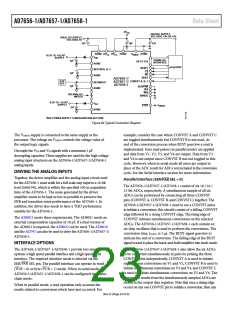
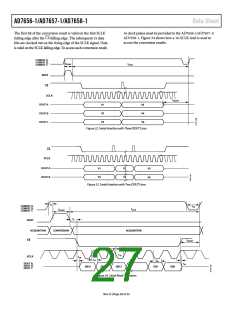
Figure 28. Typical Connection Diagram
The VDRIVE supply is connected to the same supply as the
processor. The voltage on VDRIVE controls the voltage value of
the output logic signals.
example, consider the case where CONVST A and CONVST C
are toggled simultaneously but CONVST B is not used. At
end of the conversion process when BUSY goes low a read is
implemented. Four read pulses (in parallel mode) are applied
and data from V1, V2, V5, and V6 are output. Data from V3
and V4 is not output since CONVST B was not toggled in this
cycle. However, when in serial mode all zeros are output in
place of the ADC result for ADCs not included in the conversion
cycle. See the Serial Interface section for more information.
Decouple the VDD and VSS signals with a minimum 1 µF
decoupling capacitor. These supplies are used for the high voltage
analog input structures on the AD7656-1/AD7657-1/AD7658-1
analog inputs.
DRIVING THE ANALOG INPUTS
Together, the driver amplifier and the analog input circuit used
for the AD7656-1 must settle for a full-scale step input to a 16-bit
level (0.0015%), which is within the specified 550 ns acquisition
time of the AD7656-1. The noise generated by the driver
amplifier needs to be kept as low as possible to preserve the
SNR and transition noise performance of the AD7656-1. In
addition, the driver also needs to have a THD performance
suitable for the AD7656-1.
Parallel Interface (SER/
SEL = 0)
PAR
The AD7656-1/AD7657-1/AD7658-1 consist of six 16-/14-/
12-bit ADCs, respectively. A simultaneous sample of all six
ADCs can be performed by connecting all three CONVST
pins (CONVST A, CONVST B, and CONVST C) together. The
AD7656-1/AD7657-1/AD7658-1 need to see a CONVST pulse
to initiate a conversion; this should consist of a falling CONVST
edge followed by a rising CONVST edge. The rising edge of
CONVST initiates simultaneous conversions on the selected
ADCs. The AD7656-1/AD7657-1/AD7658-1 each contain an
on-chip oscillator that is used to perform the conversions. The
conversion time, tCONV, is 3 µs. The BUSY signal goes low to
indicate the end of a conversion. The falling edge of the BUSY
signal is used to place the track-and-hold amplifier into track mode.
The AD8021 meets these requirements. The AD8021 needs an
external compensation capacitor of 10 pF. If a dual version of
the AD8021 is required, the AD8022 can be used. The AD8610
and the AD797 can also be used to drive the AD7656-1/AD7657-1/
AD7658-1.
INTERFACE OPTIONS
The AD7656-1/AD7657-1/AD7658-1 provide two interface
options: a high speed parallel interface and a high speed serial
interface. The required interface mode is selected via the
The AD7656-1/AD7657-1/AD7658-1 also allow the six ADCs
to be converted simultaneously in pairs by pulsing the three
CONVST pins independently. CONVST A is used to initiate
simultaneous conversions on V1 and V2, CONVST B is used to
initiate simultaneous conversions on V3 and V4, and CONVST C
is used to initiate simultaneous conversions on V5 and V6. The
conversion results from the simultaneously sampled ADCs are
stored in the output data registers. Note that once a rising edge
occurs on any one CONVST pin to initiate a conversion, then any
PAR
SER/
SEL pin. The parallel interface can operate in word
W
(
W
/B = 0) or byte ( /B = 1) mode. When in serial mode, the
AD7656-1/AD7657-1/AD7658-1 can be configured into daisy-
chain mode.
When in parallel mode, a read operation only accesses the
results related to conversions which have just occurred. For
Rev. D | Page 22 of 32

 ROCHESTER [ Rochester Electronics ]