AD7656-1/AD7657-1/AD7658-1
Data Sheet
SOFTWARE SELECTION OF ADCS
Table 11. Control Register Bit Function Descriptions
Bit Mnemonic Description
H
The /S SEL pin determines the source of the combination of ADCs
H
that are to be simultaneously sampled. When the /S SEL pin
is logic low, the combination of channels to be simultaneously
sampled is determined by the CONVST A, CONVST B, and
DB15 VC
DB14 VB
DB13 VA
DB12 RNGC
This bit is used to select the V5 and V6
analog inputs for the next conversion.
When this bit is set to 1, V5 and V6 are
simultaneously converted on the next
CONVST A rising edge.
H
CONVST C pins. When the /S SEL pin is logic high, the
combination of channels selected for simultaneous sampling
is determined by the contents of the DB15 to DB13 control
registers. In this mode, a write to the control register is necessary.
This bit is used to select the V3 and V4
analog inputs for the next conversion.
When this bit is set to 1, V3 and V4 are
simultaneously converted on the next
CONVST A rising edge.
The control register is an 8-bit write-only register. Data is written
CS
WR
pins and the DB[15:8] data
to this register using the
and
This bit is used to select the V1 and V2
analog inputs for the next conversion.
When this bit is set to 1, V1 and V2 are
simultaneously converted on the next
CONVST A rising edge.
pins (see Figure 31). The control register is detailed in Table 10
and Table 11. To select an ADC pair to be simultaneously sampled,
set the corresponding data line high during the write operation.
CS
This bit is used to select the analog input
range for the V5 and V6 analog inputs.
When this bit is set to 1, the 2 × VREF range
is selected for the next conversion. When
this bit is set to 0, the 4 × VREF range is
selected for the next conversion.
WR
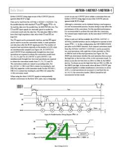
t13
t12
t11
t15
t14
DATA
DB15 TO DB8
DB11 RNGB
DB10 RNGA
This bit is used to select the analog input
range for the V3 and V4 analog inputs.
When this bit is set to 1, the 2 × VREF range
is selected for the next conversion. When
this bit is set to 0, the 4 × VREF range is
selected for the next conversion.
W
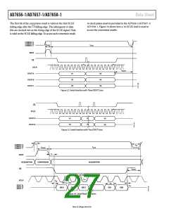
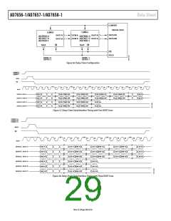
Figure 31. Parallel Interface—Write Cycle for Word Mode ( /B = 0)
The AD7656-1/AD7657-1/AD7658-1 control register allows
individual ranges to be programmed on each ADC pair. DB12
to DB10 in the control register are used to program the range
on each ADC pair.
This bit is used to select the analog input
range for the V1 and V2 analog inputs.
When this bit is set to 1, the 2 × VREF range
is selected for the next conversion. When
this bit is set to 0, the 4 × VREF range is
selected for the next conversion.
After a reset occurs on the AD7656-1/AD7657-1/AD7658-1,
the control register contains all 0s.
The CONVST A signal is used to initiate a simultaneous
conversion on the combination of channels selected via the
control register. The CONVST B and CONVST C signals can be
DB9
DB8
REFEN
This bit is used to select the internal
reference or an external reference. When
this bit is set to 0, the external reference
mode is selected. When this bit is set to 1,
the internal reference is selected.
H
tied low when operating in software mode ( /S SEL = 1). The
number of read pulses required depends on the number of
ADCs selected in the control register and on whether the
devices are operating in word or byte mode. The conversion
results are output in ascending order.
REFBUF
This bit is used to select between using the
internal reference buffers and choosing
to bypass these reference buffers. When
this bit is set to 0, the internal reference
buffers are enabled and decoupling is
required on the REFCAPx pins. When this
bit is set to 1, the internal reference buffers
are disabled and a buffered reference
should be applied to the REFCAPx pins.
During the write operation, Data Bus Bit DB15 to Data Bus Bit DB8
are bidirectional and become inputs to the control register when
RD
CS
WR
is logic high and
on DB15 through DB8 is latched into the control register when
WR
and
are logic low. The logic state
goes logic high.
Table 10. Control Register Bit Map1
DB15 DB14 DB13 DB12 DB11 DB10 DB9
DB8
VC
VB
VA
RNGC RNGB RNGA REFEN REFBUF
1 Default all 0s.
Rev. D | Page 24 of 32

 ROCHESTER [ Rochester Electronics ]