Data Sheet
AD7656-1/AD7657-1/AD7658-1
further CONVST rising edges on any of the CONVST pins are
ignored while BUSY is high.
occurs on any one CONVST pin to initiate a conversion then any
further CONVST rising edges on any of the CONVST pins are
ignored while BUSY is high.
Data can be read from the AD7656-1/AD7657-1/AD7658-1 via
Although a conversion can be initiated during a read sequence,
it is not recommended practice, because doing so may affect the
performance of the conversion. For the specified performance,
it is recommended to perform the read after the conversion.
For unused input channel pairs, tie the associated CONVST pin
CS
the parallel data bus with standard and
RD
W
signals ( /B = 0).
PAR
To read the data over the parallel bus, tie SER/
SEL low. The
input signals are internally gated to enable the
conversion result onto the data bus. The data lines DB0 to DB15
CS RD
and
CS
RD
leave their high impedance state when both
logic low.
and
are
to VDRIVE
.
If there is only an 8-bit bus available, the AD7656-1/AD7657-1/
AD7658-1 parallel interface can be configured to operate in byte
CS
RD
The
signal can be permanently tied low, and the
signal
can be used to access the conversion results. A read operation
can take place after the BUSY signal goes low. The number of
required read operations depends on the number of ADCs that
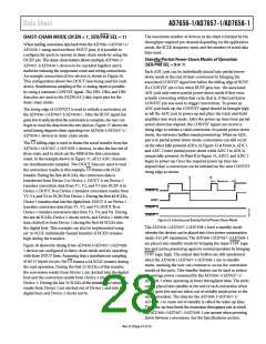
are simultaneously sampled (see Figure 29). If CONVST A
and CONVST B are simultaneously brought low, four read
operations are required to obtain the conversion results from
V1, V2, V3, and V4. If CONVST A and CONVST C are
simultaneously brought low, four read operations are required
to obtain the conversion results from V1, V2, V5, and V6.
The conversion results are output in ascending order. For
the AD7657-1, DB15 and DB14 contain two leading 0s, and
DB[13:0] output the 14-bit conversion result. For the AD7658-1,
DB[15:12] contain four leading 0s, and DB[11:0] output the
12-bit conversion result.
W
mode ( /B = 1). In this configuration, the DB7/HBEN/DCEN
pin takes on its HBEN function. Each channel conversion result
from the AD7656-1/AD7657-1/AD7658-1 can be accessed in
two read operations, with eight bits of data provided on DB15
to DB8 for each of the read operations (see Figure 30). The
HBEN pin determines whether the read operation first accesses
the high byte or the low byte of the 16-bit conversion result. To
always access the low byte first on DB15 to DB8, tie the HBEN
pin low. To always access the high byte first on DB15 to DB8, tie
the HBEN pin high. In byte mode when all three CONVST pins
are pulsed together to initiate simultaneous conversions on all six
ADCs, 12 read operations are necessary to read back the six
16-/14-/12-bit conversion results. DB[6:0] should be left
unconnected in byte mode.
When using the three CONVST signals to independently
initiate conversions on the three ADC pairs, once a rising edge
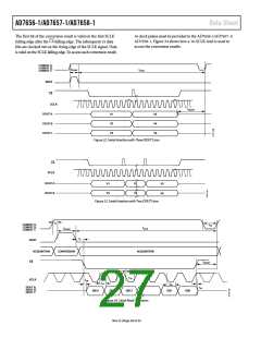
t10
CONVST A,
CONVST B,
CONVST C
tCONV
tACQ
BUSY
t4
CS
t3
t2
t5
RD
t9
t7
t6
t8
tQUIET
DATA
V1
V2
V3
V4
V5
V6
W
Figure 29. Parallel Interface Timing Diagram ( /B = 0)
CS
t4
t3
t9
t5
RD
t8
t7
t6
DB15 TO DB8
LOW BYTE
HIGH BYTE
W
Figure 30. Parallel Interface—Read Cycle for Byte Mode of Operation ( /B = 1, HBEN = 0)
Rev. D | Page 23 of 32

 ROCHESTER [ Rochester Electronics ]