AD7656-1/AD7657-1/AD7658-1
Data Sheet
THEORY OF OPERATION
CONVERTER DETAILS
and-hold amplifiers return to track mode and the acquisition
time begins.
The AD7656-1/AD7657-1/AD7658-1 are pin- and software-
compatible, reduced decoupling versions of the AD7656/AD7657/
AD7658 devices. In addition, the AD7656-1/AD7657-1/AD7658-1
are high speed, low power converters that allow the simultaneous
sampling of six on-chip ADCs. The analog inputs on the AD7656-1/
AD7657-1/AD7658-1 can accept true bipolar input signals. The
RANGE pin or RNGx bits are used to select either 4 × VREF or
2 × VREF as the input range for the next conversion.
Analog Input
The AD7656-1/AD7657-1/AD7658-1 can handle true bipolar
input voltages. The logic level on the RANGE pin or the value
written to the RNGx bits in the control register determines the
analog input range on the AD7656-1/AD7657-1/AD7658-1 for
the next conversion. When the RANGE pin or RNGx bits are 1,
the analog input range for the next conversion is 2 × VREF
When the RANGE pin or RNGx bits are 0, the analog input
range for the next conversion is 4 × VREF
.
Each AD7656-1/AD7657-1/AD7658-1 contains six SAR ADCs, six
track-and-hold amplifiers, an on-chip 2.5 V reference, reference
buffers, and high speed parallel and serial interfaces. The parts
allow the simultaneous sampling of all six ADCs when the three
CONVST pins (CONVST A, CONVST B, and CONVST C) are
tied together. Alternatively, the six ADCs can be grouped into
three pairs. Each pair has an associated CONVST signal used to
initiate simultaneous sampling on each ADC pair, on four ADCs,
or on all six ADCs. CONVST A is used to initiate simultaneous
sampling on V1 and V2, CONVST B is used to initiate simul-
taneous sampling on V3 and V4, and CONVST C is used to
initiate simultaneous sampling on V5 and V6.
.
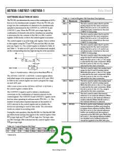
V
DD
D1
C2
R1
V1
C1
D2
V
SS
Figure 25. Equivalent Analog Input Structure
Figure 25 shows an equivalent circuit of the analog input structure
of the AD7656-1/AD7657-1/AD7658-1. The two diodes, D1 and
D2, provide ESD protection for the analog inputs. Care must be
taken to ensure that the analog input signal never exceeds the
A conversion is initiated on the AD7656-1/AD7657-1/AD7658-1
by pulsing the CONVST input. On the rising edge of CONVST,
the track-and-hold amplifier of the selected ADC pair is placed
into hold mode and the conversions are started. After the rising
edge of CONVST, the BUSY signal goes high to indicate that the
conversion is taking place. The conversion clock for the AD7656-1/
AD7657-1/AD7658-1 is internally generated, and the conversion
time for the parts is 3 µs. Any further CONVST rising edges on
either CONVST A, CONVST B or CONVST C are ignored as long
as BUSY is high. The BUSY signal returns low to indicate the end
of a conversion. On the falling edge of BUSY, the track-and-hold
amplifier returns to track mode. Data can be read from the output
register via the parallel or serial interface.
V
DD and VSS supply rails by more than 300 mV. Signals exceeding
this value cause these diodes to become forward-biased and to
start conducting current into the substrate. The maximum current
these diodes can conduct without causing irreversible damage
to the parts is 10 mA. Capacitor C1 in Figure 25 is typically
about 4 pF and can be attributed primarily to pin capacitance.
Resistor R1 is a lumped component made up of the on
resistance of a switch (that is, a track-and-hold switch). This
resistor is typically about 3.5 kΩ. Capacitor C2 is the ADC
sampling capacitor and has a capacitance of 10 pF typically.
The AD7656-1/AD7657-1/AD7658-1 require VDD and VSS dual
supplies for the high voltage analog input structures. These supplies
must be equal to or greater than the analog input range (see Table 8
for the requirements on these supplies for each analog input range).
The AD7656-1/AD7657-1/AD7658-1 require a low voltage AVCC
supply of 4.75 V to 5.25 V to power the ADC core, a DVCC supply
of 4.75 V to 5.25 V for the digital power, and a VDRIVE supply of
2.7 V to 5.25 V for the interface power.
Track-and-Hold Amplifiers
The track-and-hold amplifiers on the AD7656-1/AD7657-1/
AD7658-1 allow the ADCs to accurately convert an input
sine wave of full-scale amplitude to 16-/14-/12-bit resolution,
respectively. The input bandwidth of the track-and-hold amplifiers
is greater than the Nyquist rate of the ADC, even when the
AD7656-1/AD7657-1/AD7658-1 are operating at the maximum
throughput rate. The parts can handle input frequencies of up
to 4.5 MHz.
To meet the specified performance when using the minimum
supply voltage for the selected analog input range, it may be
necessary to reduce the throughput rate from the maximum
throughput rate.
The track-and-hold amplifiers sample their respective inputs
simultaneously on the rising edge of CONVST. The aperture time
(that is, the delay time between the external CONVST signal
actually going into hold) for the track-and-hold amplifier is 10 ns.
This is well matched across all six track-and-hold amplifiers on one
device and from device to device. This allows more than six ADCs
to be sampled simultaneously. The end of the conversion is signaled
by the falling edge of BUSY, and it is at this point that the track-
Table 8. Minimum VDD/VSS Supply Voltage Requirements
Analog Input
Range (V)
Reference
Voltage (V)
Full-Scale
Input (V)
Minimum
VDD/VSS (V)
4 × VREF
2 × VREF
2.5
2.5
10
5
10
5
Rev. D | Page 20 of 32

 ROCHESTER [ Rochester Electronics ]