Data Sheet
AD7656-1/AD7657-1/AD7658-1
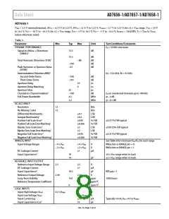
PIN CONFIGURATION AND FUNCTION DESCRIPTIONS
64 63 62 61 60 59 58 57 56 55 54 53 52 51 50 49
1
2
48
DB14/REFBUF
V6
EN/DIS
DB13
PIN 1
47
AV
AV
V5
CC
3
46
45
44
43
42
41
40
39
38
37
36
35
34
33
DB12
DB11
CC
4
5
DB10/DOUT C
DB9/DOUT B
DB8/DOUT A
DGND
AGND
AGND
V4
6
AD7656-1/AD7657-1/AD7658-1
7
TOP VIEW
(Not to Scale)
8
AV
AV
V3
CC
CC
9
V
DRIVE
10
11
12
13
14
15
16
DB7/HBEN/DCEN
DB6/SCLK
AGND
AGND
V2
DB5/DCIN A
DB4/DCIN B
DB3/DCIN C
DB2/SEL C
AV
AV
V1
CC
CC
DB1/SEL B
17 18 19 20 21 22 23 24 25 26 27 28 29 30 31 32
Figure 3. Pin Configuration
Table 7. Pin Function Descriptions
Pin No.
Mnemonic
Description
54, 56, 58
REFCAPA, REFCAPB,
REFCAPC
Reference Capacitor A, Reference Capacitor B, and Reference Capacitor C. Decoupling capacitors are
connected to these pins to decouple the reference buffer for each ADC pair. Decouple each REFCAP pin
to AGND using a 1 µF capacitor.
33, 36, 39,
42, 45, 48
V1 to V6
AGND
Analog Input 1 to Analog Input 6. These pins are single-ended analog inputs. In hardware mode,
the analog input range of these channels is determined by the RANGE pin. In software mode, it is
determined by the RNGC to RNGA bits of the control register (see Table 11).
Analog Ground. This pin is the ground reference point for all analog circuitry on the AD7656-1/
AD7657-1/AD7658-1. Refer all analog input signals and external reference signals to this pin.
Connect all AGND pins to the AGND plane of the system. The AGND and DGND voltages should
ideally be at the same potential and must not be more than 0.3 V apart, even on a transient basis.
32, 37, 38, 43,
44, 49, 52, 53,
55, 57, 59
26
DVCC
Digital Power, 4.75 V to 5.25 V. The DVCC and AVCC voltages should ideally be at the same potential
and must not be more than 0.3 V apart, even on a transient basis. Decouple this supply to DGND by
placing a 1 µF decoupling capacitor on the DVCC pin.
9
VDRIVE
Logic Power Supply Input. The voltage supplied at this pin determines the operating voltage of the
interface. This pin is nominally at the same supply as the supply of the host interface.
8, 25
DGND
Digital Ground. This is the ground reference point for all digital circuitry on the AD7656-1/AD7657-1/
AD7658-1. Connect both DGND pins to the DGND plane of a system. The DGND and AGND voltages
should ideally be at the same potential and must not be more than 0.3 V apart, even on a transient
basis.
34, 35, 40,
41, 46, 47,
50, 60
AVCC
Analog Supply Voltage, 4.75 V to 5.25 V. This is the supply voltage for the ADC cores. The AVCC and
DVCC voltages should ideally be at the same potential and must not be more than 0.3 V apart, even
on a transient basis.
21, 22, 23
CONVST C,
Conversion Start Input A, Conversion Start Input B, and Conversion Start Input C. These logic inputs
CONVST B, CONVST A are used to initiate conversions on the ADC pairs. CONVST A is used to initiate simultaneous conversions
on V1 and V2. CONVST B is used to initiate simultaneous conversions on V3 and V4. CONVST C is
used to initiate simultaneous conversions on V5 and V6. When one of these pins switches from low
to high, the track-and-hold switch on the selected ADC pair switches from track to hold, and the
conversion is initiated. These inputs can also be used to place the ADC pairs into partial power-
down mode.
Rev. D | Page 11 of 32

 ROCHESTER [ Rochester Electronics ]