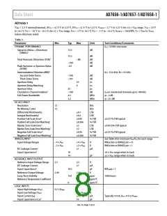
Data Sheet
AD7656-1/AD7657-1/AD7658-1
AD7658-1
VREF = 2.5 V internal/external, AVCC = 4.75 V to 5.25 V, DVCC = 4.75 V to 5.25 V, VDRIVE = 2.7 V to 5.25 V; for 4 × VREF range, VDD = 10 V
to 16.5 V, VSS = −10 V to −16.5 V; for 2 × VREF range, VDD = 5 V to 16.5 V, VSS = −5 V to −16.5 V; fSAMPLE = 250 kSPS, TA = TMIN to TMAX
,
unless otherwise noted.
Table 3.
Parameter
Min
Typ
Max
Unit
Test Conditions/Comments
DYNAMIC PERFORMANCE
fIN = 10 kHz sine wave
Signal-to-(Noise + Distortion)
(SINAD)1
73.5
73.5
dB
dB
dB
dB
dB
Total Harmonic Distortion (THD)1
−88
−100
−97
Peak Harmonic or Spurious Noise
(SFDR)1
Intermodulation Distortion (IMD)1
Second-Order Terms
Third-Order Terms
fa = 10.5 kHz, fb = 9.5 kHz
−106
−101
dB
dB
Aperture Delay
Aperture Delay Matching
10
4
ns
ns
Aperture Jitter
35
ps
Channel-to-Channel Isolation1
Full-Power Bandwidth
−100
4.5
2.2
dB
MHz
MHz
fIN on unselected channels up to 100 kHz
@ −3 dB
@ −0.1 dB
DC ACCURACY
Resolution
No Missing Codes
12
12
Bits
Bits
Differential Nonlinearity
Integral Nonlinearity1
Positive Full-Scale Error1
Positive Full-Scale Error Matching1
Bipolar Zero-Scale Error1
Bipolar Zero-Scale Error Matching1
Negative Full-Scale Error1
Negative Full-Scale Error Matching1
ANALOG INPUT
0.7
0.5
0.95
0.366
2
2
LSB
LSB
% FSR
% FSR
LSB
LSB
% FSR
% FSR
0.317% FSR typical
0.0125% FSR typical
0.317% FSR typical
0.95
0.366
See Table 8 for minimum VDD/VSS for each range
RNGx bits or RANGE pin = 0
RNGx bits or RANGE pin = 1
Input Voltage Ranges
−4 × VREF
−2 × VREF
+4 × VREF
+2 × VREF
1
V
V
µA
DC Leakage Current
Input Capacitance2
10
14
4 × VREF range when in track
2 × VREF range when in track
pF
REFERENCE INPUT/OUTPUT
Reference Input Voltage Range
DC Leakage Current
2.5
2.5
1
V
µA
pF
Input Capacitance2
18.5
150
6
REFEN/DIS = 1
1000 hours
Reference Output Voltage
Long-Term Stability
Reference Temperature Coefficient
2.49
2.51
25
V
ppm
ppm/°C
ppm/°C
LOGIC INPUTS
Input High Voltage (VINH
)
0.7 × VDRIVE
V
Input Low Voltage (VINL
Input Current (IIN)
)
0.3 × VDRIVE
10
10
V
µA
pF
Typically 10 nA, VIN = 0 V or VDRIVE
Input Capacitance (CIN)2
Rev. D | Page 7 of 32

 ROCHESTER [ Rochester Electronics ]