AD7656-1/AD7657-1/AD7658-1
Data Sheet
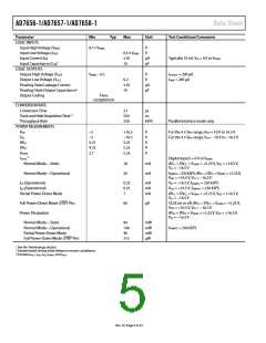
Parameter
Min
Typ
Max
Unit
Test Conditions/Comments
LOGIC OUTPUTS
Output High Voltage (VOH)
Output Low Voltage (VOL)
Floating-State Leakage Current
Floating-State Output
Capacitance2
VDRIVE − 0.2
V
V
µA
pF
ISOURCE = 200 µA
ISINK = 200 µA
0.2
10
10
Output Coding
Twos
complement
CONVERSION RATE
Conversion Time
3.1
550
250
µs
ns
kSPS
Track-and-Hold Acquisition Time1, 2
Throughput Rate
Parallel interface mode only
POWER REQUIREMENTS
VDD
VSS
AVCC
DVCC
VDRIVE
−5
−5
4.75
4.75
2.7
+16.5
−16.5
5.25
5.25
5.25
V
V
V
V
V
For the 4 × VREF range, VDD = 10 V to 16.5 V
For the 4 × VREF range, VSS= −10 V to −16.5 V
3
ITOTAL
Digital inputs = 0 V or VDRIVE
Normal Mode—Static
18
26
mA
mA
AVCC = DVCC = VDRIVE = +5.25 V, VDD = +16.5 V,
VSS =−16.5 V
fSAMPLE = 250 kSPS, AVCC = DVCC = VDRIVE = +5.25 V, VDD
+16.5 V, VSS = −16.5 V
Normal Mode—Operational
=
ISS (Operational)
IDD (Operational)
Partial Power-Down Mode
0.25
0.25
7
mA
mA
mA
VSS = −16.5 V, fSAMPLE = 250 kSPS
VDD = 16.5 V, fSAMPLE = 250 kSPS
AVCC = DVCC = VDRIVE = +5.25 V, VDD = +16.5 V,
VSS = −16.5 V
Full Power-Down Mode (STBY Pin)
Power Dissipation
60
µA
SCLK on or off, AVCC = DVCC = VDRIVE = +5.25 V,
V
DD = +16.5 V, VSS = −16.5 V
AVCC = DVCC = VDRIVE = +5.25 V, VDD = +16.5 V,
VSS = −16.5 V
Normal Mode—Static
Normal Mode—Operational
Partial Power-Down Mode
Full Power-Down Mode
(STBY Pin)
94
140
40
mW
mW
mW
µW
fSAMPLE = 250 kSPS
315
1 See the Terminology section.
2 Sample tested during initial release to ensure compliance.
3 Includes IAVCC, IVDD, IVSS, IVDRIVE, and IDVCC
.
Rev. D | Page 8 of 32

 ROCHESTER [ Rochester Electronics ]