Data Sheet
AD7656-1/AD7657-1/AD7658-1
TIMING SPECIFICATIONS
AVCC and DVCC = 4.75 V to 5.25 V, VDD = 5 V to 16.5 V, VSS = −5 V to −16.5 V, VDRIVE = 2.7 V to 5.25 V, VREF = 2.5 V internal/external,
TA = TMIN to TMAX, unless otherwise noted.
Table 4.
Limit at tMIN, tMAX
Parameter1
PARALLEL INTERFACE
tCONVERT
VDRIVE < 4.75 V
VDRIVE = 4.75 V to 5.25 V
Unit
Description
3
3
µs typ
ns min
Conversion time, internal clock
Minimum quiet time required between bus
relinquish and start of next conversion
tQUIET
150
150
tACQ
t10
t1
550
25
60
2
550
25
60
2
ns min
ns min
ns max
ms max
µs max
Acquisition time
Minimum CONVST low pulse
CONVST high to BUSY high
STBY rising edge to CONVST rising edge
Partial power-down mode
tWAKE-UP
25
25
PARALLEL READ OPERATION
t2
0
0
ns min
ns min
ns min
ns min
ns max
ns min
ns max
ns min
BUSY to RD delay
t3
0
0
CS to RD setup time
t4
0
0
CS to RD hold time
t5
45
45
10
12
6
36
36
10
12
6
RD pulse width
t6
Data access time after RD falling edge
Data hold time after RD rising edge
Bus relinquish time after RD rising edge
Minimum time between reads
t7
t8
t9
PARALLEL WRITE OPERATION
t11
t12
t13
t14
t15
15
0
15
0
ns min
ns min
ns min
ns min
ns min
WR pulse width
CS to WR setup time
5
5
CS to WR hold time
5
5
Data setup time before WR rising edge
Data hold after WR rising edge
5
5
SERIAL INTERFACE
fSCLK
t16
18
12
18
12
MHz max
ns max
Frequency of serial read clock
Delay from CS until DOUTx three-state
disabled
Data access time after SCLK rising edge/CS
falling edge
2
t17
22
22
ns max
t18
t19
t20
0.4 × tSCLK
0.4 × tSCLK
10
0.4 × tSCLK
0.4 × tSCLK
10
ns min
ns min
ns min
SCLK low pulse width
SCLK high pulse width
SCLK to data valid hold time after SCLK
falling edge
t21
18
18
ns max
CS rising edge to DOUTx high impedance
1 Sample tested during initial release to ensure compliance. All input signals are specified with tR = tF = 5 ns (10% to 90% of VDD) and timed from a voltage level of 1.6 V.
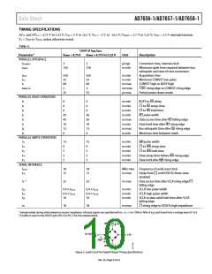
2 A buffer is used on the DOUTx pins (Pin 5 to Pin 7) for this measurement.
200µA
I
OL
TO OUTPUT
PIN
1.6V
C
L
25pF
200µA
I
OH
Figure 2. Load Circuit for Digital Output Timing Specifications
Rev. D | Page 9 of 32

 ROCHESTER [ Rochester Electronics ]